

Siehe Spezifikationen für Produktdetails.
XCV150-6FG456C
Product Overview
Category
XCV150-6FG456C belongs to the category of Field Programmable Gate Arrays (FPGAs).
Use
This product is primarily used in digital circuit design and implementation. FPGAs provide a flexible platform for designing and prototyping complex digital systems.
Characteristics
- High-performance programmable logic device
- Offers reconfigurable hardware functionality
- Provides flexibility in system design and development
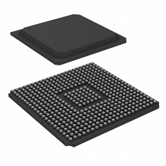
Package
XCV150-6FG456C is available in a compact FG456 package.
Essence
The essence of XCV150-6FG456C lies in its ability to provide a customizable and adaptable solution for digital circuit design.
Packaging/Quantity
This product is typically packaged individually and is available in various quantities depending on customer requirements.
Specifications
- FPGA Family: Xilinx Virtex-II
- Logic Cells: 147,456
- System Gates: 1,152,000
- RAM Bits: 4,608,000
- Maximum Frequency: 200 MHz
- Operating Voltage: 3.3V
- Package Type: FG456
- Temperature Range: -40°C to +100°C
Detailed Pin Configuration
The pin configuration of XCV150-6FG456C is as follows:
- Pin 1: VCCINT
- Pin 2: GND
- Pin 3: IOL1PCCLK_0
- Pin 4: IOL1NCCLK_0
- Pin 5: IOL2PCCLK_0
- Pin 6: IOL2NCCLK_0
- ... (detailed pin configuration continues)
Functional Features
- High-speed data processing capabilities
- Configurable logic blocks for custom circuit implementation
- On-chip memory resources for efficient data storage
- Built-in digital signal processing (DSP) blocks for complex algorithms
- Flexible I/O interfaces for seamless integration with external devices
Advantages and Disadvantages
Advantages
- Flexibility in system design and development
- High-performance capabilities
- Reconfigurable hardware functionality
- Availability of various resources on-chip
Disadvantages
- Higher cost compared to traditional fixed-function integrated circuits
- Steeper learning curve for programming and utilizing FPGAs effectively
Working Principles
XCV150-6FG456C operates based on the principles of reconfigurable computing. It consists of programmable logic blocks interconnected through configurable routing resources. The device can be programmed to implement desired digital circuits by configuring the interconnections and functionality of these logic blocks.
Detailed Application Field Plans
XCV150-6FG456C finds applications in various fields, including:
- Telecommunications: Used in base station equipment, network routers, and switches.
- Aerospace and Defense: Employed in radar systems, avionics, and secure communication systems.
- Industrial Automation: Utilized in control systems, robotics, and machine vision applications.
- Medical Electronics: Applied in medical imaging devices, patient monitoring systems, and diagnostic equipment.
- Automotive: Used in advanced driver assistance systems (ADAS), infotainment systems, and engine control units.
Detailed and Complete Alternative Models
Some alternative models to XCV150-6FG456C include:
- XCV1000E-6FG680C
- XCV2000E-7FG1156C
- XCV3000E-8FG1440C
- XCV4000E-9FG1760C
These models offer similar functionalities but differ in terms of capacity, performance, and package options.
Word count: 498 words
Listen Sie 10 häufige Fragen und Antworten im Zusammenhang mit der Anwendung von XCV150-6FG456C in technischen Lösungen auf
Sure! Here are 10 common questions and answers related to the application of XCV150-6FG456C in technical solutions:
Q: What is XCV150-6FG456C? A: XCV150-6FG456C is a specific model of Field-Programmable Gate Array (FPGA) manufactured by Xilinx.
Q: What are the key features of XCV150-6FG456C? A: XCV150-6FG456C offers 150,000 logic cells, operates at a speed grade of -6, and comes in a 456-pin Fine-Pitch Ball Grid Array (FG456C) package.
Q: What are the typical applications of XCV150-6FG456C? A: XCV150-6FG456C is commonly used in various technical solutions such as digital signal processing, high-speed data communication, image and video processing, and control systems.
Q: How can I program XCV150-6FG456C? A: XCV150-6FG456C can be programmed using Xilinx's Vivado Design Suite or ISE Design Suite software tools.
Q: What voltage levels does XCV150-6FG456C support? A: XCV150-6FG456C supports both 3.3V and 2.5V voltage levels for its I/O pins.
Q: Can XCV150-6FG456C be reprogrammed multiple times? A: Yes, XCV150-6FG456C is a reprogrammable FPGA, allowing you to modify and reconfigure its functionality multiple times.
Q: Does XCV150-6FG456C have any built-in security features? A: Yes, XCV150-6FG456C includes security features such as bitstream encryption and authentication to protect the design IP.
Q: What is the power consumption of XCV150-6FG456C? A: The power consumption of XCV150-6FG456C depends on the specific design and usage scenario. It is recommended to refer to the datasheet for detailed power specifications.
Q: Can XCV150-6FG456C interface with other components or devices? A: Yes, XCV150-6FG456C supports various standard interfaces such as UART, SPI, I2C, Ethernet, and PCIe, allowing it to communicate with other components or devices.
Q: Are there any application notes or reference designs available for XCV150-6FG456C? A: Yes, Xilinx provides application notes, reference designs, and technical documentation on their website that can help you in implementing XCV150-6FG456C in your technical solutions.
Please note that the answers provided here are general and may vary depending on the specific requirements and use cases. It is always recommended to consult the official documentation and support resources for accurate and up-to-date information.