

Siehe Spezifikationen für Produktdetails.
XCKU040-3FBVA900E
Product Overview
Category
The XCKU040-3FBVA900E belongs to the category of Field Programmable Gate Arrays (FPGAs).
Use
This FPGA is primarily used in electronic systems for various applications such as telecommunications, automotive, aerospace, and industrial automation.
Characteristics
- High-performance programmable logic device
- Offers flexibility and reconfigurability
- Provides high-speed processing capabilities
- Supports complex digital designs
- Enables rapid prototyping and development
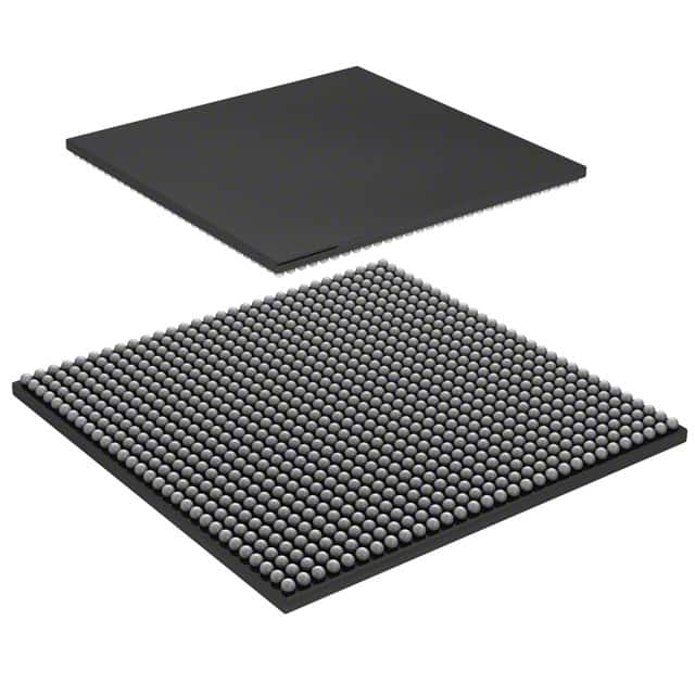
Package
The XCKU040-3FBVA900E comes in a compact package that ensures easy integration into electronic systems. It is designed to be mounted on a printed circuit board (PCB) using surface mount technology (SMT).
Essence
The essence of this FPGA lies in its ability to provide a customizable hardware platform that can be programmed to perform specific functions based on the requirements of the application.
Packaging/Quantity
The XCKU040-3FBVA900E is typically packaged in trays or reels, depending on the quantity ordered. The packaging ensures safe transportation and storage of the FPGAs.
Specifications
- Model: XCKU040-3FBVA900E
- Logic Cells: 40,000
- DSP Slices: 360
- Block RAM: 2,520 Kb
- Maximum Operating Frequency: 900 MHz
- I/O Pins: 900
- Voltage Range: 0.95V - 1.05V
- Package Type: FBVA900E
Detailed Pin Configuration
The XCKU040-3FBVA900E has a comprehensive pin configuration that allows for connectivity with external devices and components. The detailed pin configuration can be found in the product datasheet provided by the manufacturer.
Functional Features
- High-speed data processing capabilities
- Configurable logic blocks for custom functionality
- Integrated memory resources for data storage
- Flexible I/O interfaces for communication with external devices
- Built-in digital signal processing capabilities
Advantages and Disadvantages
Advantages
- Flexibility and reconfigurability
- High-performance processing capabilities
- Rapid prototyping and development
- Wide range of applications
- Integration with other electronic components
Disadvantages
- Higher cost compared to fixed-function integrated circuits
- Requires specialized knowledge for programming and configuration
- Limited power efficiency compared to dedicated hardware solutions
Working Principles
The XCKU040-3FBVA900E operates based on the principles of field programmable gate arrays. It consists of configurable logic blocks, memory elements, and I/O interfaces. The FPGA can be programmed using hardware description languages (HDLs) such as VHDL or Verilog. Once programmed, the FPGA executes the desired logic functions by routing signals through its internal resources.
Detailed Application Field Plans
The XCKU040-3FBVA900E finds extensive use in various application fields, including:
- Telecommunications: Used in network routers, switches, and base stations for high-speed data processing and protocol handling.
- Automotive: Employed in advanced driver assistance systems (ADAS), engine control units (ECUs), and infotainment systems for enhanced performance and connectivity.
- Aerospace: Utilized in satellite communication systems, avionics, and flight control systems for reliable and efficient data processing.
- Industrial Automation: Integrated into programmable logic controllers (PLCs), robotics, and industrial control systems for real-time control and automation.
Detailed and Complete Alternative Models
- XCKU060-3FBVA900E: Similar to XCKU040-3FBVA900E but with higher logic capacity and increased I/O pins.
- XCKU035-3FBVA900E: Lower-cost alternative with reduced logic capacity and I/O pins.
- XCKU100-3FBVA900E: Higher-end model with increased logic capacity, DSP slices, and memory resources.
These alternative models provide options for different project requirements and budgets while maintaining compatibility with the XCKU040-3FBVA900E in terms of architecture and programming.
In conclusion, the XCKU040-3FBVA900E is a high-performance FPGA that offers flexibility, reconfigurability, and advanced processing capabilities. Its wide range of applications, detailed pin configuration, and functional features make it a valuable component in various electronic systems.
Listen Sie 10 häufige Fragen und Antworten im Zusammenhang mit der Anwendung von XCKU040-3FBVA900E in technischen Lösungen auf
Sure! Here are 10 common questions and answers related to the application of XCKU040-3FBVA900E in technical solutions:
Question: What is the XCKU040-3FBVA900E?
Answer: The XCKU040-3FBVA900E is a field-programmable gate array (FPGA) device manufactured by Xilinx.Question: What are the key features of the XCKU040-3FBVA900E?
Answer: The key features include 40,960 logic cells, 2,520 DSP slices, 4.5 Mb of BRAM, and a maximum operating frequency of 900 MHz.Question: What are some typical applications for the XCKU040-3FBVA900E?
Answer: The XCKU040-3FBVA900E is commonly used in high-performance computing, networking, telecommunications, and aerospace applications.Question: How can I program the XCKU040-3FBVA900E?
Answer: The XCKU040-3FBVA900E can be programmed using Xilinx's Vivado Design Suite software, which supports various programming languages like VHDL and Verilog.Question: What is the power consumption of the XCKU040-3FBVA900E?
Answer: The power consumption of the XCKU040-3FBVA900E depends on the specific design and operating conditions, but it typically ranges from 5W to 15W.Question: Can I use the XCKU040-3FBVA900E in a multi-FPGA system?
Answer: Yes, the XCKU040-3FBVA900E can be used in multi-FPGA systems by connecting multiple devices together using high-speed interfaces like PCIe or Ethernet.Question: Does the XCKU040-3FBVA900E support high-speed serial communication protocols?
Answer: Yes, the XCKU040-3FBVA900E supports various high-speed serial communication protocols such as PCIe, Ethernet, and USB.Question: What is the maximum amount of external memory that can be connected to the XCKU040-3FBVA900E?
Answer: The XCKU040-3FBVA900E supports up to 4 GB of DDR4 SDRAM for external memory storage.Question: Can I use the XCKU040-3FBVA900E for real-time signal processing?
Answer: Yes, the XCKU040-3FBVA900E's high-performance DSP slices make it suitable for real-time signal processing applications.Question: Are there any development boards available for prototyping with the XCKU040-3FBVA900E?
Answer: Yes, Xilinx offers development boards like the KCU105 and VCU108, which are compatible with the XCKU040-3FBVA900E and provide a platform for rapid prototyping and evaluation.
Please note that these answers are general and may vary depending on specific design requirements and application scenarios.