

Siehe Spezifikationen für Produktdetails.
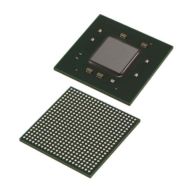
XC7K70T-2FB484I
Product Overview
Category
XC7K70T-2FB484I belongs to the category of Field Programmable Gate Arrays (FPGAs).
Use
This product is primarily used in digital logic circuits and electronic systems for various applications such as telecommunications, automotive, aerospace, and industrial automation.
Characteristics
- High-performance FPGA with advanced features
- Offers high-speed processing capabilities
- Provides flexibility for customizing digital circuits
- Supports complex algorithms and data processing tasks
- Enables rapid prototyping and system development
Package
XC7K70T-2FB484I is available in a FB484 package.
Essence
The essence of XC7K70T-2FB484I lies in its ability to provide a programmable hardware platform that allows users to implement their own digital designs and algorithms efficiently.
Packaging/Quantity
This product is typically packaged individually and is available in varying quantities depending on the manufacturer's specifications.
Specifications
- FPGA Family: Kintex-7
- Device Type: XC7K70T
- Logic Cells: 66,240
- DSP Slices: 740
- Block RAM: 4,860 Kb
- Maximum Number of User I/Os: 400
- Operating Voltage: 1.2V
- Operating Temperature Range: -40°C to +100°C
Detailed Pin Configuration
For detailed pin configuration information, please refer to the manufacturer's datasheet or user guide.
Functional Features
XC7K70T-2FB484I offers several functional features that make it a versatile FPGA for various applications:
- High-speed serial connectivity interfaces
- Integrated memory blocks for efficient data storage
- Flexible clocking resources for precise timing control
- Advanced DSP capabilities for signal processing tasks
- Configurable I/O standards for interfacing with external devices
- On-chip configuration memory for easy reprogramming
Advantages and Disadvantages
Advantages
- High-performance FPGA with advanced features
- Flexibility to implement custom digital designs
- Supports complex algorithms and data processing tasks
- Enables rapid prototyping and system development
- Wide range of applications in different industries
Disadvantages
- Relatively high power consumption compared to other programmable logic devices
- Steeper learning curve for beginners due to its complexity
- Higher cost compared to simpler programmable logic devices
Working Principles
XC7K70T-2FB484I operates based on the principles of reconfigurable hardware. It consists of a matrix of configurable logic blocks (CLBs) interconnected through programmable routing resources. Users can program the FPGA using Hardware Description Languages (HDLs) such as VHDL or Verilog to define the desired functionality.
During operation, the programmed configuration is loaded into the FPGA's internal memory, allowing it to function as a customized digital circuit. The FPGA can be reprogrammed multiple times, making it highly flexible for iterative design and testing processes.
Detailed Application Field Plans
XC7K70T-2FB484I finds extensive application in various fields, including:
- Telecommunications: Used in base stations, network routers, and communication infrastructure for high-speed data processing and signal routing.
- Automotive: Employed in automotive control systems, driver assistance systems, and infotainment systems for efficient data processing and real-time control.
- Aerospace: Utilized in satellite communication systems, onboard data processing units, and avionics for reliable and high-performance computing.
- Industrial Automation: Applied in industrial control systems, robotics, and machine vision applications for precise control and data processing.
Detailed and Complete Alternative Models
Some alternative models that offer similar capabilities to XC7K70T-2FB484I include:
- XC7K160T-2FBG676C
- XC7K325T-2FFG900I
- XC7K420T-2FFG1156E
These models belong to the same FPGA family and offer varying capacities and package options to suit different application requirements.
In conclusion, XC7K70T-2FB484I is a high-performance FPGA that provides flexibility and advanced features for implementing custom digital designs. Its wide range of applications, functional features, and programmability make it a valuable component in various industries.
Listen Sie 10 häufige Fragen und Antworten im Zusammenhang mit der Anwendung von XC7K70T-2FB484I in technischen Lösungen auf
Sure! Here are 10 common questions and answers related to the application of XC7K70T-2FB484I in technical solutions:
Q: What is XC7K70T-2FB484I? A: XC7K70T-2FB484I is a specific model of Xilinx's Kintex-7 FPGA (Field-Programmable Gate Array) family, designed for high-performance applications.
Q: What are the key features of XC7K70T-2FB484I? A: Some key features include a large number of programmable logic cells, high-speed I/O interfaces, embedded memory blocks, DSP slices, and advanced clocking capabilities.
Q: What are the typical applications of XC7K70T-2FB484I? A: XC7K70T-2FB484I is commonly used in various technical solutions such as wireless communication systems, video processing, industrial automation, medical imaging, and aerospace applications.
Q: How can XC7K70T-2FB484I be programmed? A: XC7K70T-2FB484I can be programmed using Xilinx's Vivado Design Suite, which provides a comprehensive set of tools for designing, implementing, and debugging FPGA-based systems.
Q: What is the power consumption of XC7K70T-2FB484I? A: The power consumption of XC7K70T-2FB484I depends on the specific design and operating conditions. It is recommended to refer to the datasheet or use Xilinx's Power Estimator tool for accurate power estimation.
Q: Can XC7K70T-2FB484I interface with other components or devices? A: Yes, XC7K70T-2FB484I supports various high-speed interfaces such as PCIe, Ethernet, USB, DDR3/DDR4 memory, and many more, making it compatible with a wide range of external components and devices.
Q: What is the maximum operating frequency of XC7K70T-2FB484I? A: The maximum operating frequency of XC7K70T-2FB484I depends on the specific design and implementation constraints. It is recommended to perform timing analysis using Vivado Design Suite for accurate frequency estimation.
Q: Can XC7K70T-2FB484I be used in safety-critical applications? A: Yes, XC7K70T-2FB484I can be used in safety-critical applications. However, additional measures such as redundancy, fault tolerance, and thorough verification are typically required to ensure compliance with safety standards.
Q: Are there any development boards available for XC7K70T-2FB484I? A: Yes, Xilinx offers development boards specifically designed for XC7K70T-2FB484I, such as the Kintex-7 KC705 Evaluation Kit, which provides a platform for prototyping and evaluating designs.
Q: Where can I find more information about XC7K70T-2FB484I? A: You can find more detailed information about XC7K70T-2FB484I, including datasheets, user guides, application notes, and reference designs, on Xilinx's official website or by contacting their technical support team.
Please note that the answers provided here are general and may vary depending on specific requirements and design considerations.