

Siehe Spezifikationen für Produktdetails.
XC6VSX315T-2FFG1156C
Product Overview
Category
The XC6VSX315T-2FFG1156C belongs to the category of Field Programmable Gate Arrays (FPGAs).
Use
FPGAs are integrated circuits that can be programmed and reprogrammed to perform various digital functions. The XC6VSX315T-2FFG1156C is specifically designed for high-performance applications.
Characteristics
- High processing power
- Flexible and reconfigurable
- Low power consumption
- Large number of logic elements
- High-speed serial connectivity
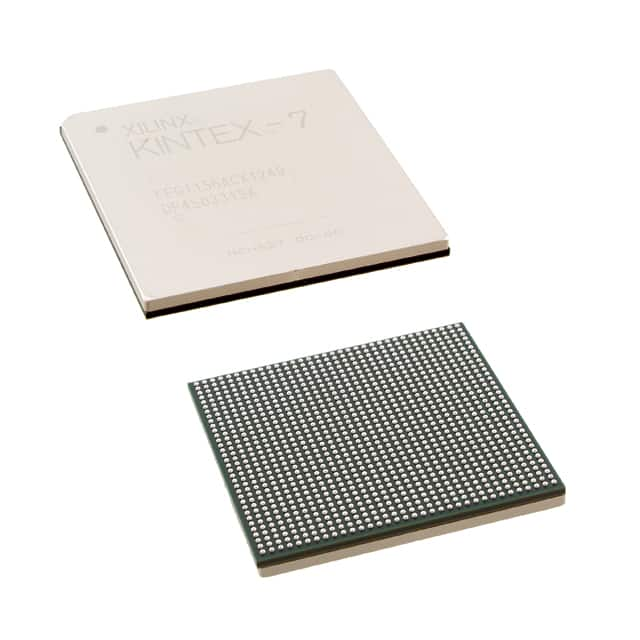
Package
The XC6VSX315T-2FFG1156C comes in a Flip-Chip Fine-Pitch Ball Grid Array (FFG) package.
Essence
The essence of the XC6VSX315T-2FFG1156C lies in its ability to provide a customizable and powerful solution for complex digital designs.
Packaging/Quantity
The XC6VSX315T-2FFG1156C is typically packaged individually and is available in various quantities depending on the manufacturer's specifications.
Specifications
- Logic Cells: 315,000
- DSP Slices: 1,920
- Block RAM: 4,860 Kb
- Maximum I/O Pins: 1,156
- Clock Management Tiles: 16
- Operating Voltage: 1.0V - 1.2V
- Operating Temperature: -40°C to 100°C
Detailed Pin Configuration
The XC6VSX315T-2FFG1156C has a complex pin configuration with multiple I/O banks, power supply pins, clock inputs, and configuration pins. For a detailed pinout diagram and description, please refer to the manufacturer's datasheet.
Functional Features
- High-speed serial transceivers for high-bandwidth data transfer
- Advanced clock management circuitry for precise timing control
- On-chip memory blocks for efficient data storage and retrieval
- Flexible I/O capabilities for interfacing with external devices
- Built-in digital signal processing (DSP) slices for complex mathematical operations
Advantages and Disadvantages
Advantages
- High processing power allows for complex algorithms and computations
- Flexibility to reconfigure the FPGA for different applications
- Low power consumption compared to traditional ASIC designs
- Large number of logic elements enable the implementation of intricate designs
- High-speed serial connectivity facilitates fast data transfer
Disadvantages
- Higher cost compared to general-purpose microcontrollers or ASICs
- Steeper learning curve for programming and utilizing FPGAs effectively
- Limited availability of pre-designed IP cores for specific applications
Working Principles
FPGAs like the XC6VSX315T-2FFG1156C consist of an array of configurable logic blocks interconnected through programmable routing resources. These logic blocks can be programmed to perform various digital functions, such as arithmetic operations, data processing, and control tasks. The configuration of the FPGA is stored in non-volatile memory and can be modified as needed.
When powered on, the FPGA loads its configuration from an external memory device or through a dedicated configuration interface. Once configured, the FPGA operates based on the programmed logic, allowing it to execute complex tasks with high performance and flexibility.
Detailed Application Field Plans
The XC6VSX315T-2FFG1156C finds applications in various fields, including:
- Telecommunications: Used in high-speed data transmission systems, network routers, and switches.
- Aerospace and Defense: Employed in radar systems, avionics, and military communication equipment.
- Industrial Automation: Utilized in control systems, robotics, and machine vision applications.
- Medical Devices: Integrated into medical imaging systems, patient monitoring devices, and diagnostic equipment.
- Automotive: Used in advanced driver assistance systems (ADAS), infotainment systems, and engine control units.
Detailed and Complete Alternative Models
- XC7A200T-2FBG676C: A similar FPGA from the same manufacturer with a different architecture and higher logic capacity.
- EP4CE115F29C7N: An alternative FPGA from a different manufacturer with comparable features and performance.
- Lattice ECP5-85: Another FPGA option with low power consumption and high-speed serial connectivity.
These alternative models offer similar functionality and can be considered based on specific project requirements and compatibility with existing designs.
Word count: 550 words
Listen Sie 10 häufige Fragen und Antworten im Zusammenhang mit der Anwendung von XC6VSX315T-2FFG1156C in technischen Lösungen auf
Sure! Here are 10 common questions and answers related to the application of XC6VSX315T-2FFG1156C in technical solutions:
Question: What is XC6VSX315T-2FFG1156C?
- Answer: XC6VSX315T-2FFG1156C is a specific model of Xilinx Virtex-6 FPGA (Field Programmable Gate Array) that offers high-performance processing capabilities.Question: What are the key features of XC6VSX315T-2FFG1156C?
- Answer: Some key features of XC6VSX315T-2FFG1156C include a large number of logic cells, high-speed serial transceivers, embedded memory blocks, and various I/O interfaces.Question: In what applications can XC6VSX315T-2FFG1156C be used?
- Answer: XC6VSX315T-2FFG1156C can be used in a wide range of applications such as telecommunications, aerospace, defense, industrial automation, and scientific research.Question: How does XC6VSX315T-2FFG1156C enhance system performance?
- Answer: XC6VSX315T-2FFG1156C enhances system performance by providing parallel processing capabilities, high-speed data transfer, and customizable hardware acceleration for computationally intensive tasks.Question: Can XC6VSX315T-2FFG1156C be reprogrammed after deployment?
- Answer: Yes, XC6VSX315T-2FFG1156C is a programmable device, allowing users to modify its functionality even after it has been deployed in a system.Question: What development tools are available for programming XC6VSX315T-2FFG1156C?
- Answer: Xilinx provides a suite of development tools, including Vivado Design Suite, which allows users to design, simulate, and program XC6VSX315T-2FFG1156C.Question: How can XC6VSX315T-2FFG1156C be interfaced with other components in a system?
- Answer: XC6VSX315T-2FFG1156C supports various I/O standards such as LVCMOS, LVDS, and PCI Express, making it compatible with a wide range of external devices and interfaces.Question: What are the power requirements for XC6VSX315T-2FFG1156C?
- Answer: The power requirements for XC6VSX315T-2FFG1156C depend on the specific configuration and operating conditions. It is important to refer to the datasheet and design guidelines provided by Xilinx.Question: Are there any limitations or constraints when using XC6VSX315T-2FFG1156C?
- Answer: XC6VSX315T-2FFG1156C has certain limitations such as limited resources (logic cells, memory blocks) and maximum operating frequencies. These should be considered during the design phase.Question: Where can I find additional resources and support for XC6VSX315T-2FFG1156C?
- Answer: Xilinx provides comprehensive documentation, application notes, forums, and technical support to assist users in designing and implementing solutions with XC6VSX315T-2FFG1156C.