

Siehe Spezifikationen für Produktdetails.
XC3S500E-4VQG100I
Product Overview
Category
The XC3S500E-4VQG100I belongs to the category of Field-Programmable Gate Arrays (FPGAs).
Use
FPGAs are integrated circuits that can be programmed and reprogrammed to perform various digital functions. The XC3S500E-4VQG100I is specifically designed for applications requiring high-performance logic capacity and flexibility.
Characteristics
- High logic capacity: The XC3S500E-4VQG100I offers a large number of configurable logic blocks, allowing for complex digital designs.
- Flexibility: With its programmable nature, this FPGA provides the ability to implement custom logic functions and adapt to changing requirements.
- Low power consumption: The XC3S500E-4VQG100I is designed to minimize power consumption, making it suitable for battery-powered devices.
- Fast performance: This FPGA offers high-speed operation, enabling efficient execution of complex algorithms.
Package
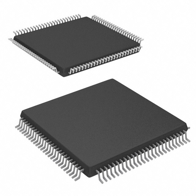
The XC3S500E-4VQG100I comes in a Quad Flat No-Lead (QFN) package, which provides a compact form factor and ease of integration into electronic systems.
Essence
The essence of the XC3S500E-4VQG100I lies in its ability to provide a flexible and high-capacity solution for implementing digital logic functions.
Packaging/Quantity
The XC3S500E-4VQG100I is typically packaged in reels or trays, with each reel or tray containing a specific quantity of FPGAs. The exact packaging and quantity may vary depending on the supplier.
Specifications
- Logic Capacity: 500,000 system gates
- Number of Configurable Logic Blocks: 1,536
- Maximum User I/Os: 332
- Operating Voltage: 1.2V
- Maximum Operating Frequency: 400 MHz
Detailed Pin Configuration
The XC3S500E-4VQG100I has a total of 100 pins, each serving a specific purpose in the FPGA's operation. The pin configuration includes input/output pins, power supply pins, and configuration pins. A detailed pinout diagram can be found in the product datasheet.
Functional Features
High-Level Integration
The XC3S500E-4VQG100I offers a high level of integration, allowing for the implementation of complex digital systems on a single chip. This reduces the need for external components and simplifies system design.
Reconfigurability
One of the key features of FPGAs is their reprogrammable nature. The XC3S500E-4VQG100I can be reconfigured multiple times, enabling rapid prototyping, design iteration, and field upgrades without the need for hardware changes.
Embedded Memory
This FPGA includes embedded memory blocks, which can be used to store data or program code. The presence of on-chip memory enhances system performance and reduces the need for external memory components.
High-Speed Interfaces
The XC3S500E-4VQG100I supports various high-speed interfaces, such as DDR3, PCIe, and Ethernet. These interfaces enable seamless integration with other system components and facilitate fast data transfer.
Advantages and Disadvantages
Advantages
- Flexibility in implementing custom logic functions.
- High logic capacity for complex designs.
- Low power consumption, suitable for battery-powered devices.
- Reconfigurability allows for rapid prototyping and design iteration.
- High-speed interfaces enable efficient data transfer.
Disadvantages
- Steeper learning curve compared to traditional fixed-function integrated circuits.
- Higher cost compared to dedicated application-specific integrated circuits (ASICs) for large-scale production.
Working Principles
The XC3S500E-4VQG100I operates based on the principles of reconfigurable logic. It consists of an array of configurable logic blocks interconnected through programmable routing resources. The FPGA can be programmed using a hardware description language (HDL) to define the desired digital logic functions and interconnections.
During operation, the FPGA's configuration memory is loaded with the user-defined bitstream, which determines the functionality of the device. The internal interconnects and logic elements are then configured accordingly, allowing the FPGA to perform the desired digital operations.
Detailed Application Field Plans
The XC3S500E-4VQG100I finds applications in various fields, including:
- Communications: Used in wireless base stations, routers, and network switches for high-speed data processing and protocol handling.
- Industrial Automation: Employed in control systems, motor drives, and robotics for real-time control and signal processing.
- Aerospace and Defense: Utilized in radar systems, avionics, and military communication equipment for high-performance signal processing and encryption.
- Medical Devices
Listen Sie 10 häufige Fragen und Antworten im Zusammenhang mit der Anwendung von XC3S500E-4VQG100I in technischen Lösungen auf
Sure! Here are 10 common questions and answers related to the application of XC3S500E-4VQG100I in technical solutions:
Question: What is XC3S500E-4VQG100I?
- Answer: XC3S500E-4VQG100I is a field-programmable gate array (FPGA) from Xilinx, which offers programmable logic and digital signal processing capabilities.Question: What are the key features of XC3S500E-4VQG100I?
- Answer: Some key features include 500,000 system gates, 36Kbits of block RAM, 500MHz maximum operating frequency, and 100-pin Quad Flat No-Lead (QFN) package.Question: What are the typical applications of XC3S500E-4VQG100I?
- Answer: XC3S500E-4VQG100I is commonly used in applications such as industrial automation, telecommunications, automotive electronics, medical devices, and aerospace systems.Question: How can I program XC3S500E-4VQG100I?
- Answer: XC3S500E-4VQG100I can be programmed using Xilinx's Vivado Design Suite or ISE Design Suite software tools, which allow you to write and compile your FPGA design code.Question: What programming languages are supported for XC3S500E-4VQG100I?
- Answer: XC3S500E-4VQG100I supports various hardware description languages (HDLs) like VHDL and Verilog, which are commonly used for FPGA designs.Question: Can XC3S500E-4VQG100I interface with other components or devices?
- Answer: Yes, XC3S500E-4VQG100I supports various communication protocols like SPI, I2C, UART, and Ethernet, allowing it to interface with other components or devices in your system.Question: What are the power requirements for XC3S500E-4VQG100I?
- Answer: XC3S500E-4VQG100I typically operates at a voltage range of 1.14V to 1.26V, with a maximum power consumption of around 1.5W.Question: Can XC3S500E-4VQG100I be reprogrammed multiple times?
- Answer: Yes, XC3S500E-4VQG100I is a reprogrammable FPGA, which means you can modify and reprogram its configuration multiple times as per your application requirements.Question: Are there any development boards available for XC3S500E-4VQG100I?
- Answer: Yes, Xilinx provides development boards like the Spartan-3E Starter Kit, which includes XC3S500E-4VQG100I, allowing you to prototype and test your designs.Question: Where can I find technical documentation and support for XC3S500E-4VQG100I?
- Answer: You can find technical documentation, datasheets, application notes, and support resources on Xilinx's official website or by contacting their customer support team.
Please note that the answers provided here are general and may vary depending on specific requirements and use cases. It's always recommended to refer to the official documentation and consult with experts for accurate information.