

Siehe Spezifikationen für Produktdetails.
XC3S400A-4FGG400I
Product Overview
Category
The XC3S400A-4FGG400I belongs to the category of Field Programmable Gate Arrays (FPGAs).
Use
FPGAs are integrated circuits that can be programmed and reprogrammed to perform various digital functions. The XC3S400A-4FGG400I is specifically designed for applications requiring high-performance logic and signal processing capabilities.
Characteristics
- High-performance FPGA with advanced features
- Flexible and reconfigurable design
- Offers a large number of programmable logic cells and input/output blocks
- Supports various communication protocols and interfaces
- Provides high-speed data processing capabilities
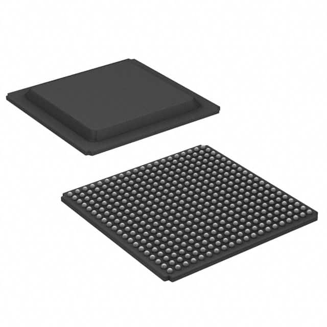
Package
The XC3S400A-4FGG400I comes in a compact and durable package, ensuring easy handling and protection during transportation and installation.
Essence
The essence of the XC3S400A-4FGG400I lies in its ability to provide a customizable and versatile solution for complex digital circuit designs. It allows users to implement their desired functionality by programming the FPGA according to their specific requirements.
Packaging/Quantity
The XC3S400A-4FGG400I is typically packaged individually and is available in various quantities depending on the customer's needs.
Specifications
- FPGA Family: Spartan-3A
- Logic Cells: 400,000
- System Gates: 40,000
- Block RAM: 1,152 Kbits
- DSP Slices: 96
- Maximum Frequency: 400 MHz
- Operating Voltage: 1.2V
- Package Type: FG(G)400
- Temperature Range: Industrial (-40°C to +85°C)
Detailed Pin Configuration
The XC3S400A-4FGG400I has a comprehensive pin configuration, allowing for seamless integration into various circuit designs. For a detailed pin configuration diagram, please refer to the manufacturer's datasheet.
Functional Features
- High-performance logic and signal processing capabilities
- Flexible and reconfigurable design for customization
- Support for various communication protocols and interfaces
- Efficient utilization of programmable resources
- Low power consumption
- Built-in security features for protecting intellectual property
Advantages and Disadvantages
Advantages
- Versatile and customizable solution for complex digital circuit designs
- High-performance capabilities for demanding applications
- Flexibility in adapting to changing requirements
- Cost-effective compared to custom ASIC designs
- Shorter development time compared to traditional hardware designs
Disadvantages
- Higher power consumption compared to dedicated hardware solutions
- Limited resources may restrict the complexity of designs
- Steeper learning curve for programming and utilizing FPGAs effectively
Working Principles
The XC3S400A-4FGG400I operates based on the principles of reconfigurable computing. It consists of an array of configurable logic blocks interconnected through programmable routing resources. The FPGA can be programmed using Hardware Description Languages (HDLs) such as VHDL or Verilog to define the desired functionality. Upon programming, the FPGA configures its internal resources to implement the specified logic and signal processing operations.
Detailed Application Field Plans
The XC3S400A-4FGG400I finds applications in various fields, including:
- Telecommunications: Used in base stations, routers, and network switches for high-speed data processing and protocol handling.
- Aerospace and Defense: Employed in radar systems, avionics, and military communication equipment for their high-performance and reconfigurable nature.
- Industrial Automation: Utilized in control systems, robotics, and machine vision applications for real-time processing and control.
- Medical Devices: Integrated into medical imaging systems, patient monitoring devices, and diagnostic equipment for their processing capabilities.
- Automotive: Used in advanced driver assistance systems (ADAS), infotainment systems, and engine control units (ECUs) for efficient data processing.
Detailed and Complete Alternative Models
- XC3S200A-4FGG400I: A lower-capacity variant of the same FPGA family, suitable for less demanding applications.
- XC6SLX150-2FGG484C: A higher-performance FPGA from a different family, offering increased logic capacity and additional features.
- XC7A35T-1CPG236C: An entry-level FPGA with lower power consumption, ideal for cost-sensitive applications.
These alternative models provide options with varying capacities, performance levels, and price points to cater to different application requirements.
Word count: 550 words
Listen Sie 10 häufige Fragen und Antworten im Zusammenhang mit der Anwendung von XC3S400A-4FGG400I in technischen Lösungen auf
Sure! Here are 10 common questions and answers related to the application of XC3S400A-4FGG400I in technical solutions:
Q: What is XC3S400A-4FGG400I? A: XC3S400A-4FGG400I is a field-programmable gate array (FPGA) from Xilinx, which offers high-performance digital logic capabilities for various technical applications.
Q: What are the key features of XC3S400A-4FGG400I? A: Some key features include 400,000 system gates, 400 MHz maximum operating frequency, 4-input look-up tables, 36Kbits of block RAM, and 16 DSP slices.
Q: What are the typical applications of XC3S400A-4FGG400I? A: XC3S400A-4FGG400I is commonly used in applications such as telecommunications, industrial automation, medical devices, automotive systems, and aerospace engineering.
Q: How can I program XC3S400A-4FGG400I? A: XC3S400A-4FGG400I can be programmed using Xilinx's Vivado Design Suite or ISE Design Suite software tools, which allow you to create and implement your digital designs.
Q: What is the power supply requirement for XC3S400A-4FGG400I? A: The recommended power supply voltage for XC3S400A-4FGG400I is 1.14V to 1.26V, with a maximum current consumption of 500mA.
Q: Can XC3S400A-4FGG400I interface with other components or devices? A: Yes, XC3S400A-4FGG400I supports various communication interfaces such as SPI, I2C, UART, and Ethernet, allowing it to interface with other components or devices in your system.
Q: What is the maximum operating temperature for XC3S400A-4FGG400I? A: The maximum junction temperature for XC3S400A-4FGG400I is 100°C, but it is recommended to operate within a temperature range of -40°C to 85°C for reliable performance.
Q: Can XC3S400A-4FGG400I be reprogrammed multiple times? A: Yes, XC3S400A-4FGG400I is a reprogrammable FPGA, which means you can modify and reconfigure its logic multiple times to suit different application requirements.
Q: Are there any development boards available for XC3S400A-4FGG400I? A: Yes, Xilinx offers development boards like the Spartan-3A Evaluation Kit, which provide a platform for prototyping and testing designs using XC3S400A-4FGG400I.
Q: Where can I find more technical documentation and support for XC3S400A-4FGG400I? A: You can find detailed technical documentation, application notes, and support resources on Xilinx's official website, including forums and community platforms for assistance from experts and fellow users.
Please note that the answers provided here are general and may vary depending on specific design requirements and implementation details. It is always recommended to refer to the official documentation and consult with experts for accurate and up-to-date information.