

Siehe Spezifikationen für Produktdetails.
XA7S25-2CSGA225I
Product Overview
Category
The XA7S25-2CSGA225I belongs to the category of Field Programmable Gate Arrays (FPGAs).
Use
FPGAs are integrated circuits that can be programmed and reprogrammed to perform various digital functions. The XA7S25-2CSGA225I is specifically designed for high-performance applications that require programmable logic.
Characteristics
- High-performance FPGA with advanced programmable logic capabilities.
- Offers a wide range of features and functionalities.
- Provides flexibility in designing and implementing complex digital systems.
- Supports rapid prototyping and development of custom digital circuits.
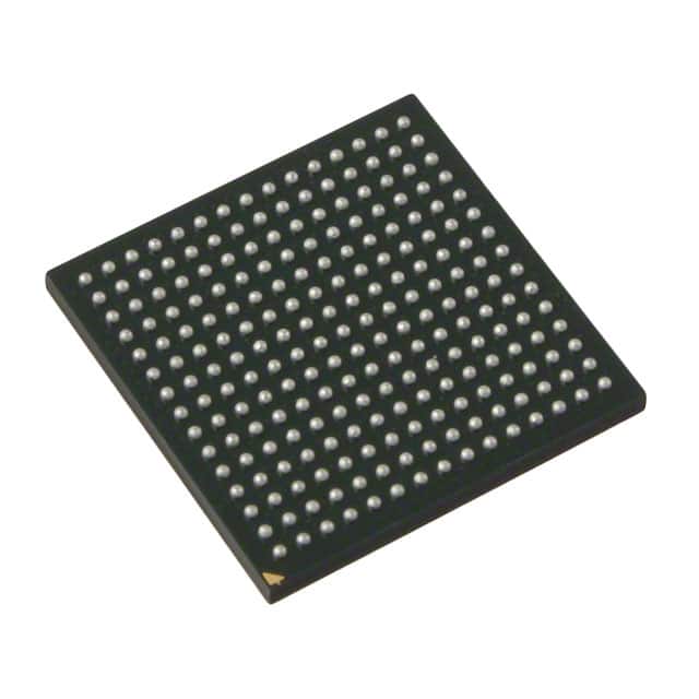
Package
The XA7S25-2CSGA225I comes in a compact and durable package, ensuring easy handling and protection during transportation and installation.
Essence
The essence of the XA7S25-2CSGA225I lies in its ability to provide a versatile and customizable solution for digital circuit design and implementation.
Packaging/Quantity
The XA7S25-2CSGA225I is typically packaged individually and is available in varying quantities depending on the specific requirements of the user.
Specifications
- FPGA Family: Xilinx 7 Series
- Logic Cells: 25,000
- System Gates: 52,160
- Block RAM: 1,080 Kb
- DSP Slices: 80
- I/O Pins: 225
- Operating Voltage: 1.2V
- Maximum Frequency: 550 MHz
- Package Type: CSGA225
Detailed Pin Configuration
The XA7S25-2CSGA225I has a total of 225 I/O pins, each serving a specific purpose in the overall functionality of the FPGA. The detailed pin configuration can be found in the product datasheet provided by the manufacturer.
Functional Features
- High-performance programmable logic for complex digital circuit design.
- Flexible and customizable architecture to meet specific application requirements.
- Support for various communication protocols and interfaces.
- Advanced clock management and synchronization capabilities.
- On-chip memory resources for efficient data storage and retrieval.
- Built-in DSP slices for implementing signal processing algorithms.
- Integrated power management features for optimized energy consumption.
Advantages and Disadvantages
Advantages
- Versatile and flexible solution for digital circuit design.
- Rapid prototyping and development capabilities.
- High-performance and advanced programmable logic.
- Wide range of I/O pins for interfacing with external devices.
- Efficient power management features.
Disadvantages
- Steep learning curve for beginners due to the complexity of FPGA programming.
- Higher cost compared to traditional fixed-function integrated circuits.
- Limited availability of alternative models with similar specifications.
Working Principles
The XA7S25-2CSGA225I operates based on the principles of reconfigurable computing. It consists of an array of configurable logic blocks interconnected through programmable routing resources. The user can program the FPGA using a Hardware Description Language (HDL) to define the desired functionality and interconnections of the logic blocks. Upon configuration, the FPGA executes the programmed logic, enabling the implementation of complex digital systems.
Detailed Application Field Plans
The XA7S25-2CSGA225I finds applications in various fields, including:
- Telecommunications: Used in base stations, network routers, and switches for high-speed data processing and protocol handling.
- Aerospace and Defense: Employed in radar systems, avionics, and military communication equipment for their high-performance and flexibility.
- Industrial Automation: Utilized in control systems, robotics, and machine vision applications for real-time data processing and control.
- Medical Devices: Integrated into medical imaging systems, patient monitoring devices, and laboratory equipment for their computational capabilities.
- Automotive: Used in advanced driver assistance systems (ADAS), infotainment systems, and engine control units (ECUs) for enhanced functionality.
Detailed and Complete Alternative Models
- XA7S50-2CSGA225I: A higher-capacity FPGA from the same Xilinx 7 Series family, offering 50,000 logic cells and increased system gates.
- XA7S15-2CSGA225I: A lower-capacity FPGA from the same Xilinx 7 Series family, suitable for applications with less demanding requirements.
- XA7S100-2CSGA225I: A higher-capacity FPGA from the same Xilinx 7 Series family, providing 100,000 logic cells and expanded memory resources.
These alternative models offer varying capacities and features to cater to different application needs within the Xilinx 7 Series FPGA family.
Word count: 590 words
Listen Sie 10 häufige Fragen und Antworten im Zusammenhang mit der Anwendung von XA7S25-2CSGA225I in technischen Lösungen auf
Sure! Here are 10 common questions and answers related to the application of XA7S25-2CSGA225I in technical solutions:
Q: What is XA7S25-2CSGA225I? A: XA7S25-2CSGA225I is a specific model of Field Programmable Gate Array (FPGA) manufactured by Xilinx.
Q: What are the key features of XA7S25-2CSGA225I? A: Some key features of XA7S25-2CSGA225I include 25,920 logic cells, 1,620 Kbits of block RAM, 90 DSP slices, and support for various I/O standards.
Q: What are the typical applications of XA7S25-2CSGA225I? A: XA7S25-2CSGA225I is commonly used in applications such as industrial automation, automotive electronics, telecommunications, medical devices, and aerospace systems.
Q: How can XA7S25-2CSGA225I be programmed? A: XA7S25-2CSGA225I can be programmed using Hardware Description Languages (HDLs) like VHDL or Verilog, or through Xilinx's Vivado Design Suite.
Q: Can XA7S25-2CSGA225I be reprogrammed after deployment? A: Yes, XA7S25-2CSGA225I is a reprogrammable FPGA, allowing for flexibility and updates even after deployment.
Q: What are the power requirements for XA7S25-2CSGA225I? A: The power requirements for XA7S25-2CSGA225I typically range from 1.2V to 3.3V, depending on the specific design and configuration.
Q: Does XA7S25-2CSGA225I support high-speed interfaces? A: Yes, XA7S25-2CSGA225I supports various high-speed interfaces such as PCIe, Ethernet, USB, and DDR3/DDR4 memory interfaces.
Q: Can XA7S25-2CSGA225I be used in safety-critical applications? A: Yes, XA7S25-2CSGA225I can be used in safety-critical applications by following appropriate design practices and adhering to relevant safety standards.
Q: Are there any development boards available for XA7S25-2CSGA225I? A: Yes, Xilinx offers development boards like the Zynq-7000 SoC ZC702 Evaluation Kit that include XA7S25-2CSGA225I for prototyping and development purposes.
Q: Where can I find technical documentation and support for XA7S25-2CSGA225I? A: Technical documentation, datasheets, application notes, and support resources for XA7S25-2CSGA225I can be found on Xilinx's official website or through their customer support channels.
Please note that the specific details and answers may vary based on the manufacturer's documentation and guidelines.