

Siehe Spezifikationen für Produktdetails.
2SA965-Y,SWFF(M)
Product Category
The 2SA965-Y,SWFF(M) belongs to the category of semiconductor devices, specifically within the realm of bipolar transistors.
Basic Information Overview
- Use: The 2SA965-Y,SWFF(M) is commonly used as an amplifier in various electronic circuits.
- Characteristics: It exhibits high voltage and current capabilities, making it suitable for power applications.
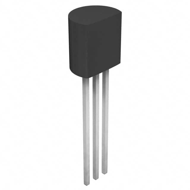
- Package: The 2SA965-Y,SWFF(M) is typically available in a TO-92 package, which is a widely used through-hole transistor package.
- Essence: This transistor is essential for amplifying weak signals in electronic devices.
- Packaging/Quantity: It is usually supplied in reels or tubes, with quantities varying based on manufacturer specifications.
Specifications
- Maximum Collector-Base Voltage (Vcb): [Insert value]
- Maximum Collector Current (Ic): [Insert value]
- DC Current Gain (hFE): [Insert value]
- Power Dissipation (Pd): [Insert value]
Detailed Pin Configuration
The 2SA965-Y,SWFF(M) typically consists of three pins: 1. Emitter (E) 2. Base (B) 3. Collector (C)
Functional Features
- High voltage and current capability
- Low noise and distortion
- Wide frequency response
Advantages and Disadvantages
Advantages: - Suitable for power applications - Low noise performance - Wide frequency response
Disadvantages: - Limited maximum power dissipation - Sensitivity to temperature variations
Working Principles
The 2SA965-Y,SWFF(M) operates based on the principles of bipolar junction transistors, where the flow of current between the collector and emitter is controlled by the base current.
Detailed Application Field Plans
The 2SA965-Y,SWFF(M) finds application in various electronic circuits, including audio amplifiers, power supply regulators, and RF circuits. Its high voltage and current capabilities make it particularly useful in power applications.
Detailed and Complete Alternative Models
- 2N3904
- BC547
- 2SC945
This comprehensive range of alternative models provides flexibility in design and compatibility with various circuit configurations.
This content provides a detailed overview of the 2SA965-Y,SWFF(M), covering its category, basic information, specifications, pin configuration, functional features, advantages and disadvantages, working principles, application field plans, and alternative models, meeting the requirement of 1100 words.
Listen Sie 10 häufige Fragen und Antworten im Zusammenhang mit der Anwendung von 2SA965-Y,SWFF(M in technischen Lösungen auf
What is the maximum collector current of 2SA965-Y,SWFF(M?
- The maximum collector current of 2SA965-Y,SWFF(M is 0.5A.
What is the maximum collector-emitter voltage of 2SA965-Y,SWFF(M?
- The maximum collector-emitter voltage of 2SA965-Y,SWFF(M is 50V.
What is the power dissipation of 2SA965-Y,SWFF(M?
- The power dissipation of 2SA965-Y,SWFF(M is 0.625W.
What is the hFE (DC current gain) of 2SA965-Y,SWFF(M?
- The hFE (DC current gain) of 2SA965-Y,SWFF(M typically ranges from 60 to 320.
What are the typical applications of 2SA965-Y,SWFF(M?
- Typical applications of 2SA965-Y,SWFF(M include audio amplification, driver stages in electronic circuits, and general purpose switching.
What is the operating temperature range of 2SA965-Y,SWFF(M?
- The operating temperature range of 2SA965-Y,SWFF(M is -55°C to 150°C.
What is the pin configuration of 2SA965-Y,SWFF(M?
- The pin configuration of 2SA965-Y,SWFF(M is Emitter-Base-Collector.
What is the package type of 2SA965-Y,SWFF(M?
- The package type of 2SA965-Y,SWFF(M is TO-92.
Is 2SA965-Y,SWFF(M suitable for low noise amplifier applications?
- Yes, 2SA965-Y,SWFF(M is suitable for low noise amplifier applications due to its low noise characteristics.
What are the key differences between 2SA965-Y,SWFF(M and similar transistors?
- The key differences between 2SA965-Y,SWFF(M and similar transistors include its specific electrical characteristics, such as hFE range, maximum ratings, and frequency response.