

Siehe Spezifikationen für Produktdetails.
TXS03121DRLR
Product Overview
- Category: Integrated Circuit (IC)
- Use: Signal Level Shifter
- Characteristics: High-speed, Bi-directional, Voltage Translation
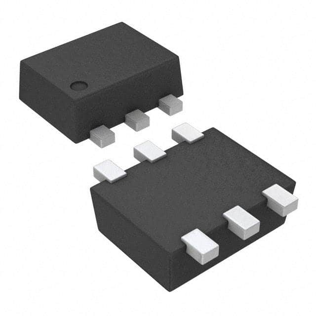
- Package: 8-pin VSSOP
- Essence: Translates voltage levels between different logic families
- Packaging/Quantity: Tape and Reel, 3000 units per reel
Specifications
- Supply Voltage: 1.2V to 3.6V
- Logic Voltage Levels: 1.2V to 3.6V
- Data Rate: Up to 100 Mbps
- Number of Channels: 1
- Input/Output Compatibility: CMOS, TTL, LVCMOS, LVTTL
Detailed Pin Configuration
The TXS03121DRLR has the following pin configuration:
- OE (Output Enable)
- A1 (Channel A Input/Output)
- GND (Ground)
- B1 (Channel B Input/Output)
- VCCA (Voltage Supply for Channel A)
- VCCB (Voltage Supply for Channel B)
- B2 (Channel B Input/Output)
- A2 (Channel A Input/Output)
Functional Features
- Bi-directional voltage translation between two logic levels
- Automatic direction sensing eliminates the need for direction control signals
- Supports multiple logic families such as CMOS, TTL, LVCMOS, and LVTTL
- High-speed data transmission up to 100 Mbps
- Low power consumption
- ESD protection on all pins
Advantages and Disadvantages
Advantages: - Simplifies interfacing between different logic families - Eliminates the need for additional level shifting components - Automatic direction sensing simplifies system design - High-speed data transmission capability
Disadvantages: - Limited to a single channel - Not suitable for applications requiring multiple voltage translations simultaneously
Working Principles
The TXS03121DRLR is a bidirectional voltage level shifter that allows seamless translation between different logic families. It utilizes a combination of MOSFETs and control circuitry to automatically sense the direction of data flow and perform the necessary voltage translation.
When the OE pin is low, the device is enabled, and the input on one side (A1/A2) is translated to the output on the other side (B1/B2) based on the logic voltage levels specified by VCCA and VCCB. The device supports both high-to-low and low-to-high voltage translation.
Detailed Application Field Plans
The TXS03121DRLR can be used in various applications where voltage translation between different logic families is required. Some potential application fields include:
- Microcontroller interfacing with different peripheral devices
- Communication interfaces such as UART, SPI, and I2C
- Level shifting in mixed-signal systems
- Battery-powered devices with multiple voltage domains
- Industrial automation and control systems
Detailed and Complete Alternative Models
- TXS0108EPWR: 8-bit Bidirectional Voltage-Level Translator with Automatic Direction Sensing
- SN74LVC1T45DBVR: Single-Bit Dual-Supply Bus Transceiver with Configurable Voltage Translation and 3-State Outputs
- PCA9306DCUR: Dual Bi-Directional I2C-Bus and SMBus Voltage-Level Translator
These alternative models offer similar functionality and can be considered as alternatives to the TXS03121DRLR depending on specific requirements and design constraints.
Word count: 447 words
Listen Sie 10 häufige Fragen und Antworten im Zusammenhang mit der Anwendung von TXS03121DRLR in technischen Lösungen auf
Sure! Here are 10 common questions and answers related to the application of TXS03121DRLR in technical solutions:
Question: What is TXS03121DRLR?
Answer: TXS03121DRLR is a specific model of a digital multiplexer/demultiplexer IC (Integrated Circuit) used for signal routing and control in various technical applications.Question: What is the operating voltage range of TXS03121DRLR?
Answer: The operating voltage range of TXS03121DRLR is typically between 1.65V and 3.6V.Question: How many channels does TXS03121DRLR have?
Answer: TXS03121DRLR has three channels, allowing it to handle multiple input/output signals simultaneously.Question: What is the maximum data rate supported by TXS03121DRLR?
Answer: TXS03121DRLR supports a maximum data rate of up to 100 Mbps, making it suitable for high-speed data transmission applications.Question: Can TXS03121DRLR be used for bidirectional communication?
Answer: Yes, TXS03121DRLR supports bidirectional communication, allowing data to be transmitted in both directions through its channels.Question: What is the power supply current requirement for TXS03121DRLR?
Answer: The power supply current requirement for TXS03121DRLR is typically around 1 mA, making it energy-efficient.Question: Is TXS03121DRLR compatible with different logic families?
Answer: Yes, TXS03121DRLR is compatible with various logic families such as CMOS, TTL, and LVCMOS, ensuring compatibility with different systems.Question: Can TXS03121DRLR be used in automotive applications?
Answer: Yes, TXS03121DRLR is designed to meet automotive industry standards and can be used in automotive applications.Question: Does TXS03121DRLR have built-in ESD protection?
Answer: Yes, TXS03121DRLR has built-in ESD (Electrostatic Discharge) protection, ensuring robustness and reliability in harsh environments.Question: What package options are available for TXS03121DRLR?
Answer: TXS03121DRLR is available in different package options, such as VQFN and TSSOP, providing flexibility for various PCB layouts and assembly processes.
Please note that the answers provided here are general and may vary depending on the specific datasheet and manufacturer's specifications of TXS03121DRLR.