

Siehe Spezifikationen für Produktdetails.
SN74LVC1G08DRY2
Product Overview
Category
The SN74LVC1G08DRY2 belongs to the category of integrated circuits (ICs).
Use
This IC is commonly used as a logic gate, specifically an AND gate.
Characteristics
- Low-voltage CMOS technology
- High-speed operation
- Wide operating voltage range
- Small package size
- Low power consumption
Package
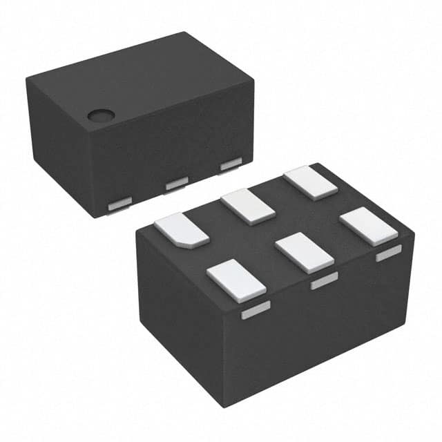
The SN74LVC1G08DRY2 is available in a small SOT-23 package.
Essence
The essence of this product lies in its ability to perform logical AND operations on input signals.
Packaging/Quantity
The SN74LVC1G08DRY2 is typically packaged in reels or tubes and is available in large quantities for industrial applications.
Specifications
- Supply Voltage Range: 1.65V to 5.5V
- Input Voltage Range: 0V to VCC
- Output Voltage Range: 0V to VCC
- Operating Temperature Range: -40°C to +125°C
- Propagation Delay: 3.8ns (typical)
- Maximum Quiescent Current: 10μA
Detailed Pin Configuration
The SN74LVC1G08DRY2 has a total of three pins:
- GND (Ground): Connected to the ground reference potential.
- A (Input): Input pin for the first logic signal.
- Y (Output): Output pin for the logical AND result.
Functional Features
The SN74LVC1G08DRY2 offers the following functional features:
- Logical AND operation: The IC performs a logical AND operation on the input signals applied to pin A.
- High-speed operation: With a propagation delay of only 3.8ns, it enables fast processing of input signals.
- Wide operating voltage range: The IC can operate within a voltage range of 1.65V to 5.5V, making it compatible with various systems.
- Low power consumption: The SN74LVC1G08DRY2 consumes minimal power, making it suitable for battery-powered devices.
Advantages and Disadvantages
Advantages
- Small package size allows for space-saving designs.
- High-speed operation enables efficient signal processing.
- Wide operating voltage range provides flexibility in system integration.
- Low power consumption prolongs battery life in portable applications.
Disadvantages
- Limited number of input pins restricts the complexity of logic operations that can be performed.
- Single-channel design may not be suitable for applications requiring multiple logic gates.
Working Principles
The SN74LVC1G08DRY2 operates based on CMOS technology. It consists of transistors that form a logical AND gate. When a logical high (1) is applied to both input pins A, the output pin Y will produce a logical high (1). Otherwise, if any of the input pins receives a logical low (0), the output pin will produce a logical low (0).
Detailed Application Field Plans
The SN74LVC1G08DRY2 finds applications in various fields, including:
- Digital electronics: Used in microcontrollers, processors, and other digital circuits to perform logical AND operations.
- Communication systems: Employed in data transmission and reception circuits to process signals.
- Industrial automation: Integrated into control systems for logical decision-making processes.
- Automotive electronics: Utilized in vehicle control units for signal processing and decision-making.
Detailed and Complete Alternative Models
- SN74LVC1G08DCKR: Similar to SN74LVC1G08DRY2 but available in a different package (SC-70).
- SN74LVC1G08DBVR: Similar to SN74LVC1G08DRY2 but available in a different package (SOT-23).
- SN74LVC1G08DRLR: Similar to SN74LVC1G08DRY2 but available in a different package (TSOT-5).
These alternative models offer similar functionality and characteristics, providing options for different packaging requirements.
In conclusion, the SN74LVC1G08DRY2 is a versatile logic gate IC that performs logical AND operations. Its small size, high-speed operation, wide voltage range, and low power consumption make it suitable for various applications in digital electronics, communication systems, industrial automation, and automotive electronics. Alternative models with different packaging options are also available, providing flexibility in design and integration.
Listen Sie 10 häufige Fragen und Antworten im Zusammenhang mit der Anwendung von SN74LVC1G08DRY2 in technischen Lösungen auf
Sure! Here are 10 common questions and answers related to the application of SN74LVC1G08DRY2 in technical solutions:
Q1: What is SN74LVC1G08DRY2? A1: SN74LVC1G08DRY2 is a single 2-input AND gate IC (integrated circuit) manufactured by Texas Instruments.
Q2: What is the voltage supply range for SN74LVC1G08DRY2? A2: The voltage supply range for SN74LVC1G08DRY2 is typically between 1.65V and 5.5V.
Q3: What is the maximum output current of SN74LVC1G08DRY2? A3: The maximum output current of SN74LVC1G08DRY2 is approximately 32mA.
Q4: Can SN74LVC1G08DRY2 be used as a level shifter? A4: Yes, SN74LVC1G08DRY2 can be used as a level shifter to convert signals between different voltage levels.
Q5: What is the propagation delay of SN74LVC1G08DRY2? A5: The propagation delay of SN74LVC1G08DRY2 is typically around 3.8ns.
Q6: Can SN74LVC1G08DRY2 be used in battery-powered applications? A6: Yes, SN74LVC1G08DRY2 is suitable for battery-powered applications due to its low power consumption.
Q7: Is SN74LVC1G08DRY2 compatible with both CMOS and TTL logic levels? A7: Yes, SN74LVC1G08DRY2 is compatible with both CMOS (3.3V) and TTL (5V) logic levels.
Q8: Can SN74LVC1G08DRY2 be used in high-speed applications? A8: Yes, SN74LVC1G08DRY2 is capable of operating at high speeds, making it suitable for high-speed applications.
Q9: What is the package type of SN74LVC1G08DRY2? A9: SN74LVC1G08DRY2 is available in a small SOT-23-5 package.
Q10: Can SN74LVC1G08DRY2 be used in automotive applications? A10: Yes, SN74LVC1G08DRY2 is qualified for automotive applications and meets the necessary standards.
Please note that these answers are general and may vary depending on specific datasheet specifications and application requirements.