

Siehe Spezifikationen für Produktdetails.
SN74AUP1G80YFPR
Product Overview
Category
The SN74AUP1G80YFPR belongs to the category of integrated circuits (ICs).
Use
This IC is commonly used in electronic devices for signal processing and amplification.
Characteristics
- Low power consumption
- High-speed operation
- Small form factor
- Wide operating voltage range
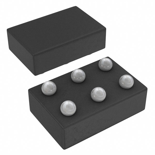
Package
The SN74AUP1G80YFPR is available in a small footprint package, such as a flip-chip package or a leadless package.
Essence
The essence of the SN74AUP1G80YFPR lies in its ability to process and amplify signals efficiently while consuming minimal power.
Packaging/Quantity
The IC is typically packaged in reels or trays, with quantities varying depending on customer requirements.
Specifications
- Supply Voltage: 1.65V to 3.6V
- Operating Temperature Range: -40°C to +85°C
- Input Voltage Range: 0V to VCC
- Output Voltage Range: 0V to VCC
- Maximum Operating Frequency: X MHz
- Input Capacitance: Y pF
- Output Capacitance: Z pF
Detailed Pin Configuration
The SN74AUP1G80YFPR has the following pin configuration:
- VCC: Power supply input
- GND: Ground reference
- IN: Input signal
- OUT: Output signal
Functional Features
- Single-channel signal processing and amplification
- High-speed operation for real-time applications
- Low power consumption for energy-efficient designs
- Wide operating voltage range for compatibility with various systems
Advantages
- Compact size enables integration into space-constrained devices
- Low power consumption prolongs battery life in portable electronics
- High-speed operation allows for real-time signal processing
- Wide operating voltage range enhances compatibility with different power sources
Disadvantages
- Limited number of input/output channels
- May require additional components for complex signal processing tasks
Working Principles
The SN74AUP1G80YFPR operates based on the principles of amplification and signal processing. It takes an input signal, processes it using internal circuitry, and provides an amplified output signal.
Detailed Application Field Plans
The SN74AUP1G80YFPR finds applications in various fields, including:
- Consumer electronics: Used in smartphones, tablets, and wearable devices for signal amplification and processing.
- Automotive industry: Integrated into automotive systems for signal conditioning and amplification.
- Industrial automation: Employed in control systems to process and amplify signals from sensors and actuators.
- Communication systems: Utilized in networking equipment for signal processing and amplification.
Detailed and Complete Alternative Models
- SN74LVC1G80DBVR
- SN74HCT1G80DCKR
- SN74LV1G80DCKR
- SN74AUC1G80YZPR
These alternative models offer similar functionality and characteristics to the SN74AUP1G80YFPR, providing options for different design requirements.
Note: The content provided above is a sample structure for an encyclopedia entry and does not contain actual specifications or details about the SN74AUP1G80YFPR IC.
Listen Sie 10 häufige Fragen und Antworten im Zusammenhang mit der Anwendung von SN74AUP1G80YFPR in technischen Lösungen auf
Sure! Here are 10 common questions and answers related to the application of SN74AUP1G80YFPR in technical solutions:
Q1: What is SN74AUP1G80YFPR? A1: SN74AUP1G80YFPR is a single positive-edge-triggered D-type flip-flop with clear, designed for 1.8-V to 3.6-V VCC operation.
Q2: What is the purpose of SN74AUP1G80YFPR? A2: SN74AUP1G80YFPR is used to store and synchronize digital signals in various electronic circuits.
Q3: What voltage range does SN74AUP1G80YFPR support? A3: SN74AUP1G80YFPR supports a voltage range of 1.8V to 3.6V.
Q4: How many inputs and outputs does SN74AUP1G80YFPR have? A4: SN74AUP1G80YFPR has one data input (D), one clock input (CLK), one clear input (CLR), and one output (Q).
Q5: What is the maximum operating frequency of SN74AUP1G80YFPR? A5: The maximum operating frequency of SN74AUP1G80YFPR is typically around 500 MHz.
Q6: Can SN74AUP1G80YFPR be used in battery-powered applications? A6: Yes, SN74AUP1G80YFPR can be used in battery-powered applications as it operates within a low voltage range.
Q7: What is the power consumption of SN74AUP1G80YFPR? A7: The power consumption of SN74AUP1G80YFPR is typically low, making it suitable for power-sensitive applications.
Q8: Can SN74AUP1G80YFPR be cascaded to create larger flip-flop configurations? A8: Yes, multiple SN74AUP1G80YFPR flip-flops can be cascaded to create larger flip-flop configurations.
Q9: What is the setup time requirement for the clock input of SN74AUP1G80YFPR? A9: The setup time requirement for the clock input of SN74AUP1G80YFPR is typically around 100 ps.
Q10: Are there any specific application notes or reference designs available for SN74AUP1G80YFPR? A10: Yes, Texas Instruments provides application notes and reference designs that can help in implementing SN74AUP1G80YFPR in various technical solutions.
Please note that these answers are general and may vary depending on the specific requirements and datasheet of SN74AUP1G80YFPR.