

Siehe Spezifikationen für Produktdetails.
SN74AUC32374ZKER
Product Overview
Category
The SN74AUC32374ZKER belongs to the category of integrated circuits (ICs).
Use
This IC is commonly used in digital systems for data storage and transfer.
Characteristics
- Low power consumption
- High-speed operation
- Wide operating voltage range
- Compatibility with various logic families
Package
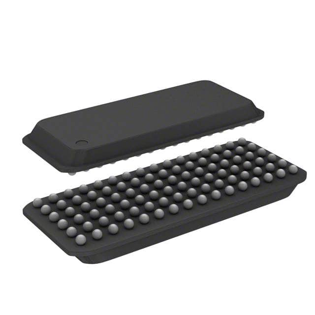
The SN74AUC32374ZKER is available in a small form factor package, such as a 48-pin TSSOP (Thin Shrink Small Outline Package).
Essence
The essence of this product lies in its ability to store and transfer digital data efficiently within electronic systems.
Packaging/Quantity
The SN74AUC32374ZKER is typically packaged in reels or tubes, with a quantity of 250 units per reel/tube.
Specifications
- Supply Voltage: 1.2V - 3.6V
- Operating Temperature Range: -40°C to +85°C
- Input/Output Type: Tri-State
- Number of Bits: 32
- Logic Family: AUC
Detailed Pin Configuration
The SN74AUC32374ZKER has a total of 48 pins, which are assigned specific functions. The pin configuration is as follows:
- Pin 1: Output Enable (OE)
- Pin 2: Data Input D0
- Pin 3: Data Input D1
- Pin 4: Data Input D2
- Pin 5: Data Input D3
- Pin 6: Data Input D4
- Pin 7: Data Input D5
- Pin 8: Data Input D6
- Pin 9: Data Input D7
- Pin 10: Data Input D8
- Pin 11: Data Input D9
- Pin 12: Data Input D10
- Pin 13: Data Input D11
- Pin 14: Data Input D12
- Pin 15: Data Input D13
- Pin 16: Data Input D14
- Pin 17: Data Input D15
- Pin 18: Output Q0
- Pin 19: Output Q1
- Pin 20: Output Q2
- Pin 21: Output Q3
- Pin 22: Output Q4
- Pin 23: Output Q5
- Pin 24: Output Q6
- Pin 25: Output Q7
- Pin 26: Output Q8
- Pin 27: Output Q9
- Pin 28: Output Q10
- Pin 29: Output Q11
- Pin 30: Output Q12
- Pin 31: Output Q13
- Pin 32: Output Q14
- Pin 33: Output Q15
- Pin 34: Output Enable (OE)
- Pin 35: Clock (CLK)
- Pin 36: Clock Enable (CE)
- Pin 37: Master Reset (MR)
- Pin 38: Data Input D16
- Pin 39: Data Input D17
- Pin 40: Data Input D18
- Pin 41: Data Input D19
- Pin 42: Data Input D20
- Pin 43: Data Input D21
- Pin 44: Data Input D22
- Pin 45: Data Input D23
- Pin 46: Data Input D24
- Pin 47: Data Input D25
- Pin 48: Data Input D26
Functional Features
- Tri-State Outputs: The SN74AUC32374ZKER features tri-state outputs, allowing for efficient data transfer and sharing between multiple devices.
- High-Speed Operation: This IC operates at high speeds, enabling rapid data processing and transmission.
- Low Power Consumption: With its low power consumption characteristics, the SN74AUC32374ZKER helps conserve energy in electronic systems.
- Wide Operating Voltage Range: The IC can operate within a wide voltage range, providing flexibility in various applications.
Advantages and Disadvantages
Advantages
- Efficient data storage and transfer capabilities
- Compatibility with different logic families
- Low power consumption
- High-speed operation
Disadvantages
- Limited number of bits (32)
- Requires careful handling due to small form factor package
Working Principles
The SN74AUC32374ZKER functions as a latch or flip-flop, storing digital data and allowing it to be transferred between different parts of a digital system. It operates based on clock signals and control inputs, which enable the storage and retrieval of data.
#
Listen Sie 10 häufige Fragen und Antworten im Zusammenhang mit der Anwendung von SN74AUC32374ZKER in technischen Lösungen auf
Sure! Here are 10 common questions and answers related to the application of SN74AUC32374ZKER in technical solutions:
Q: What is SN74AUC32374ZKER? A: SN74AUC32374ZKER is a specific model of octal D-type flip-flop with 3-state outputs, manufactured by Texas Instruments.
Q: What is the purpose of SN74AUC32374ZKER? A: SN74AUC32374ZKER is used for storing and transferring digital data in various electronic systems.
Q: What is the operating voltage range of SN74AUC32374ZKER? A: The operating voltage range of SN74AUC32374ZKER is typically between 0.8V and 2.7V.
Q: How many flip-flops are there in SN74AUC32374ZKER? A: SN74AUC32374ZKER consists of 8 individual D-type flip-flops.
Q: What is the maximum clock frequency supported by SN74AUC32374ZKER? A: SN74AUC32374ZKER can operate at a maximum clock frequency of 200 MHz.
Q: Can SN74AUC32374ZKER be used in both synchronous and asynchronous applications? A: Yes, SN74AUC32374ZKER can be used in both synchronous and asynchronous applications.
Q: What is the output drive strength of SN74AUC32374ZKER? A: The output drive strength of SN74AUC32374ZKER is typically 12 mA.
Q: Does SN74AUC32374ZKER support 3-state outputs? A: Yes, SN74AUC32374ZKER supports 3-state outputs, allowing multiple devices to share a common bus.
Q: What is the package type of SN74AUC32374ZKER? A: SN74AUC32374ZKER is available in a 48-pin BGA (Ball Grid Array) package.
Q: Can SN74AUC32374ZKER be used in automotive applications? A: Yes, SN74AUC32374ZKER is qualified for automotive applications and meets the necessary standards.
Please note that these answers are general and may vary depending on the specific datasheet and application requirements.