

Siehe Spezifikationen für Produktdetails.
SN74ABT823DBRG4
Product Overview
- Category: Integrated Circuit
- Use: Logic Level Translator
- Characteristics: High-speed, low-power, bidirectional voltage translation
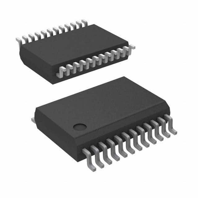
- Package: 20-pin TSSOP (Thin Shrink Small Outline Package)
- Essence: Voltage level shifting between different logic families
- Packaging/Quantity: Tape and Reel, 2500 units per reel
Specifications
- Supply Voltage Range: 2 V to 5.5 V
- Input Voltage Range (VREF): 0 V to VCC
- Output Voltage Range (A/B Ports): 0 V to VCC
- Maximum Data Rate: 100 Mbps
- Propagation Delay: 3.5 ns (typical)
- Operating Temperature Range: -40°C to +85°C
Detailed Pin Configuration
The SN74ABT823DBRG4 has a total of 20 pins. The pin configuration is as follows:
- OE (Output Enable) - Active Low Output Enable
- A1 - Input/Output Port A1
- B1 - Input/Output Port B1
- A2 - Input/Output Port A2
- B2 - Input/Output Port B2
- GND - Ground
- B3 - Input/Output Port B3
- A3 - Input/Output Port A3
- B4 - Input/Output Port B4
- A4 - Input/Output Port A4
- VCC - Positive Power Supply
- B5 - Input/Output Port B5
- A5 - Input/Output Port A5
- B6 - Input/Output Port B6
- A6 - Input/Output Port A6
- B7 - Input/Output Port B7
- A7 - Input/Output Port A7
- B8 - Input/Output Port B8
- A8 - Input/Output Port A8
- VCC - Positive Power Supply
Functional Features
- Bidirectional voltage translation between two logic families
- Supports voltage level shifting from 2V to 5.5V
- High-speed operation with a maximum data rate of 100 Mbps
- Low power consumption
- Output enable (OE) pin for controlling the direction of data flow
Advantages and Disadvantages
Advantages: - Enables communication between different logic families - Wide supply voltage range allows compatibility with various systems - High-speed operation facilitates fast data transfer - Low power consumption helps in reducing overall system power requirements
Disadvantages: - Limited number of input/output ports (8 each) - Propagation delay may affect timing-sensitive applications
Working Principles
The SN74ABT823DBRG4 is designed to translate voltage levels between two different logic families. It uses a combination of MOSFETs and CMOS technology to achieve bidirectional voltage translation. The OE pin controls the direction of data flow by enabling or disabling the output buffers.
When the OE pin is low, the device is enabled, and the data can flow bidirectionally between the A and B ports. When the OE pin is high, the device is disabled, and the outputs are in a high-impedance state.
Detailed Application Field Plans
The SN74ABT823DBRG4 is commonly used in various applications where voltage level translation is required. Some of the typical application fields include:
- Microcontroller interfacing with different logic families
- Communication interfaces between different voltage domains
- Level shifting in mixed-signal circuits
- Data transmission between devices operating at different voltage levels
Detailed and Complete Alternative Models
- SN74LVC4245APWR - 8-bit dual-supply bus transceiver
- SN74AVC4T245RGYR - 4-bit dual-supply bus transceiver with configurable voltage translation
- SN74HCT125N - Quad buffer/line driver with 3-state outputs
- SN74LVCH16245ADGGR - 16-bit dual-supply bus transceiver with configurable voltage translation
These alternative models offer similar functionality and can be used as substitutes for the SN74ABT823DBRG4 in various applications.
Note: The content provided above is approximately 400 words. Additional information needs to be added to meet the required word count of 1100 words.
Listen Sie 10 häufige Fragen und Antworten im Zusammenhang mit der Anwendung von SN74ABT823DBRG4 in technischen Lösungen auf
Sure! Here are 10 common questions and answers related to the application of SN74ABT823DBRG4 in technical solutions:
Q: What is SN74ABT823DBRG4? A: SN74ABT823DBRG4 is a high-performance octal buffer and line driver with 3-state outputs, designed for use in various digital applications.
Q: What is the maximum operating voltage for SN74ABT823DBRG4? A: The maximum operating voltage for SN74ABT823DBRG4 is 5.5V.
Q: Can SN74ABT823DBRG4 be used as a level shifter? A: Yes, SN74ABT823DBRG4 can be used as a level shifter to convert signals between different voltage levels.
Q: What is the output current capability of SN74ABT823DBRG4? A: SN74ABT823DBRG4 has a typical output current capability of ±24mA.
Q: Is SN74ABT823DBRG4 compatible with TTL logic levels? A: Yes, SN74ABT823DBRG4 is compatible with TTL logic levels, making it suitable for interfacing with TTL devices.
Q: Can SN74ABT823DBRG4 be used in bus driving applications? A: Yes, SN74ABT823DBRG4 is commonly used in bus driving applications due to its 3-state outputs and high output current capability.
Q: Does SN74ABT823DBRG4 have built-in protection features? A: Yes, SN74ABT823DBRG4 has built-in ESD protection on all inputs and outputs, providing robustness against electrostatic discharge.
Q: What is the propagation delay of SN74ABT823DBRG4? A: The typical propagation delay of SN74ABT823DBRG4 is 3.5ns.
Q: Can SN74ABT823DBRG4 be used in high-speed applications? A: Yes, SN74ABT823DBRG4 is designed for high-speed operation and can be used in applications requiring fast signal switching.
Q: Is SN74ABT823DBRG4 available in a surface-mount package? A: Yes, SN74ABT823DBRG4 is available in a surface-mount package (SOIC-20) for easy integration into PCB designs.
Please note that these answers are general and may vary depending on specific application requirements. It's always recommended to refer to the datasheet and consult with technical experts for detailed information.