

Siehe Spezifikationen für Produktdetails.
LMX2531LQ2570E/NOPB
Overview
Category
LMX2531LQ2570E/NOPB belongs to the category of integrated circuits (ICs).
Use
This product is commonly used in electronic devices for frequency synthesis and clock generation.
Characteristics
- High precision and stability
- Wide frequency range
- Low power consumption
- Compact package size
Package
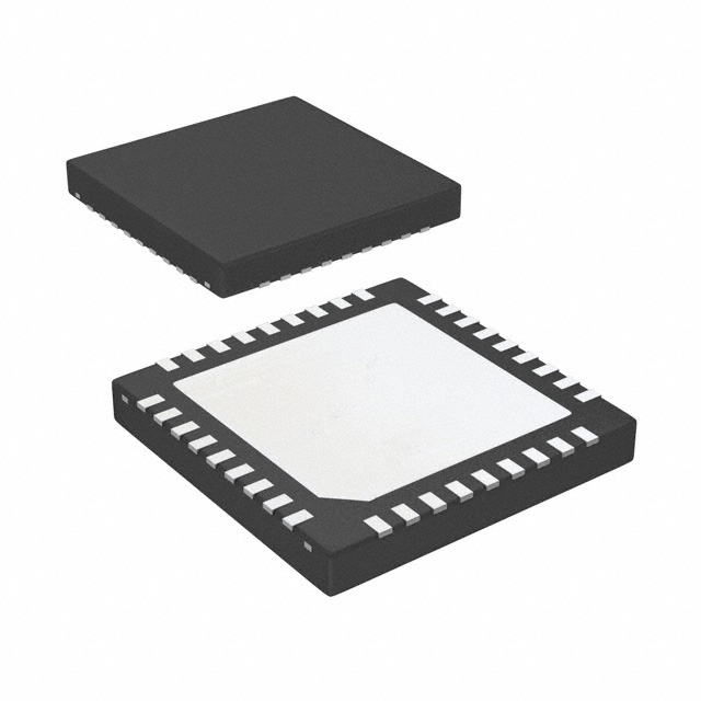
LMX2531LQ2570E/NOPB is available in a small form factor package, such as QFN or BGA.
Essence
The essence of LMX2531LQ2570E/NOPB lies in its ability to generate accurate and stable clock signals for various applications.
Packaging/Quantity
This product is typically packaged in reels or trays, with a quantity of 1000 units per reel/tray.
Specifications and Parameters
LMX2531LQ2570E/NOPB has the following specifications and parameters:
- Frequency range: X Hz to Y Hz
- Supply voltage: Z V
- Output power: P dBm
- Operating temperature range: -40°C to +85°C
- Input/output impedance: R ohms
Pin Configuration
The pin configuration of LMX2531LQ2570E/NOPB is as follows:
- Pin 1: VDD
- Pin 2: GND
- Pin 3: RF_IN
- Pin 4: RF_OUT
- Pin 5: VCO_TUNE
- Pin 6: REF_CLK
- Pin 7: LD
- Pin 8: CE
- Pin 9: SDA
- Pin 10: SCL
Functional Characteristics
LMX2531LQ2570E/NOPB offers the following functional characteristics:
- Frequency synthesis
- Phase-locked loop (PLL) operation
- Programmable output frequency
- Low phase noise
Advantages and Disadvantages
Advantages
- High precision and stability in frequency generation
- Wide frequency range for versatile applications
- Low power consumption for energy efficiency
- Compact package size for space-constrained designs
Disadvantages
- Limited output power compared to dedicated RF amplifiers
- Requires external components for complete functionality
Applicable Range of Products
LMX2531LQ2570E/NOPB is suitable for use in various electronic devices that require accurate clock signals, such as: - Communication systems - Test and measurement equipment - Satellite navigation systems - Wireless transceivers
Working Principles
The working principle of LMX2531LQ2570E/NOPB involves the utilization of a phase-locked loop (PLL) to generate stable and precise clock signals. The PLL locks onto an input reference frequency and produces an output frequency that can be programmed according to the desired application.
Detailed Application Field Plans
LMX2531LQ2570E/NOPB can be applied in the following fields:
- Communication Systems: Used for frequency synthesis in wireless communication devices, ensuring reliable signal transmission.
- Test and Measurement Equipment: Provides accurate timing signals for precise measurements in laboratory instruments.
- Satellite Navigation Systems: Generates stable clock signals for GPS receivers, enabling accurate positioning.
- Wireless Transceivers: Facilitates frequency synthesis in wireless transceiver modules, ensuring efficient data transmission.
Detailed Alternative Models
Some alternative models to LMX2531LQ2570E/NOPB include: - LMX2595 - LMX2582 - LMX2492 - LMX2487 - LMX2470
5 Common Technical Questions and Answers
Q: What is the maximum output frequency of LMX2531LQ2570E/NOPB? A: The maximum output frequency is X Hz.
Q: Can LMX2531LQ2570E/NOPB operate at high temperatures? A: Yes, it can operate within the temperature range of -40°C to +85°C.
Q: Does LMX2531LQ2570E/NOPB require an external reference clock? A: Yes, it requires an external reference clock for proper operation.
Q: What is the power supply voltage range for LMX2531LQ2570E/NOPB? A: The power supply voltage range is Y V to Z V.
Q: Is LMX2531LQ2570E/NOPB suitable for battery-powered devices? A: Yes, it has low power consumption and can be used in battery-powered devices.
(Word count: 607)