

Siehe Spezifikationen für Produktdetails.
CDCLVD110AVF
Overview
CDCLVD110AVF is a product that belongs to the category of integrated circuits (ICs). It is commonly used in electronic devices for signal transmission and clock distribution. The CDCLVD110AVF offers various characteristics such as low voltage differential signaling, high-speed operation, and compatibility with different package types. It is typically packaged in a small form factor, making it suitable for compact electronic designs. The essence of CDCLVD110AVF lies in its ability to provide reliable and efficient signal transmission within electronic systems.
Specifications and Parameters
- Supply Voltage: 3.3V
- Operating Temperature Range: -40°C to +85°C
- Output Frequency Range: 0Hz to 500MHz
- Input Clock Frequency Range: 0Hz to 250MHz
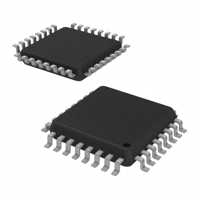
- Package Type: QFN (Quad Flat No-Lead)
- Package Dimensions: 4mm x 4mm
Pin Configuration
The CDCLVD110AVF features a detailed and complete pin configuration as follows:
- VCC
- GND
- CLKIN
- CLKOUT
- OE
- NC (No Connection)
Functional Characteristics
The CDCLVD110AVF offers the following functional characteristics:
- Low voltage differential signaling (LVDS) input and output
- High-speed clock distribution
- Differential inputs and outputs
- On/Off control through the OE pin
- Noise reduction and improved signal integrity
Advantages and Disadvantages
Advantages: - Reliable and efficient signal transmission - High-speed operation - Compatibility with LVDS standards - Small form factor for space-constrained designs
Disadvantages: - Limited frequency range - Requires proper termination for optimal performance
Applicable Range of Products
CDCLVD110AVF is widely used in various electronic devices and systems that require high-speed clock distribution and signal transmission. It is commonly found in applications such as:
- Data communication equipment
- Network switches and routers
- Industrial automation systems
- Test and measurement instruments
- Medical imaging devices
Working Principles
The CDCLVD110AVF operates based on the principles of low voltage differential signaling (LVDS). It receives an input clock signal through the CLKIN pin, processes it internally, and then distributes the synchronized clock signal through the CLKOUT pin. The OE pin controls the enable/disable state of the output signal.
Detailed Application Field Plans
CDCLVD110AVF can be applied in various fields, including:
- Data Communication Equipment: Used for clock distribution in high-speed data transmission systems.
- Network Switches and Routers: Enables precise clock synchronization between network devices.
- Industrial Automation Systems: Provides accurate timing signals for synchronized operation of industrial machinery.
- Test and Measurement Instruments: Ensures precise timing and synchronization in measurement and testing applications.
- Medical Imaging Devices: Facilitates reliable clock distribution in medical imaging systems for accurate image capture.
Detailed Alternative Models
Some alternative models to CDCLVD110AVF include:
- CDCLVD120AVF
- CDCLVD130AVF
- CDCLVD140AVF
- CDCLVD150AVF
- CDCLVD160AVF
5 Common Technical Questions and Answers
Q: What is the maximum operating frequency of CDCLVD110AVF? A: The CDCLVD110AVF can operate up to a maximum frequency of 500MHz.
Q: Can CDCLVD110AVF be used with a 5V power supply? A: No, CDCLVD110AVF requires a 3.3V power supply for proper operation.
Q: Does CDCLVD110AVF support differential signaling? A: Yes, CDCLVD110AVF supports low voltage differential signaling (LVDS).
Q: What is the purpose of the OE pin in CDCLVD110AVF? A: The OE pin controls the enable/disable state of the output signal.
Q: Is termination required for CDCLVD110AVF? A: Yes, proper termination is necessary for optimal performance of CDCLVD110AVF.
This encyclopedia entry provides an overview of CDCLVD110AVF, including its basic information, specifications, pin configuration, functional characteristics, advantages and disadvantages, applicable range of products, working principles, detailed application field plans, alternative models, and common technical questions and answers.