Siehe Spezifikationen für Produktdetails.

Encyclopedia Entry: 74ALVCH16334DGGRE4
Product Overview
Category
The 74ALVCH16334DGGRE4 belongs to the category of integrated circuits (ICs). Specifically, it falls under the category of digital logic ICs.
Use
This product is commonly used in electronic devices and systems for signal processing and data manipulation. It serves as a buffer/line driver, providing high-speed and reliable signal transmission between different components of a circuit.
Characteristics
- High-speed operation: The 74ALVCH16334DGGRE4 is designed to operate at high frequencies, making it suitable for applications that require fast data transfer.
- Low power consumption: This IC is optimized for low power consumption, making it energy-efficient and suitable for battery-powered devices.
- Wide voltage range: It can operate within a wide voltage range, typically from 1.65V to 3.6V, allowing compatibility with various systems.
- Robust design: The 74ALVCH16334DGGRE4 is built to withstand harsh environmental conditions and provide reliable performance.
Package and Quantity
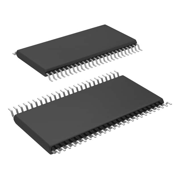
The 74ALVCH16334DGGRE4 is available in a surface-mount package known as TSSOP (Thin Shrink Small Outline Package). It consists of 48 pins arranged in a compact form factor. The product is typically sold in reels or tubes containing multiple units.
Essence
The essence of the 74ALVCH16334DGGRE4 lies in its ability to ensure efficient and reliable signal transmission within electronic circuits. By acting as a buffer/line driver, it helps prevent signal degradation and distortion, ensuring accurate data transfer.
Specifications
- Logic family: ALVCH
- Number of channels: 16
- Input/output type: Non-inverting
- Supply voltage range: 1.65V to 3.6V
- Operating temperature range: -40°C to +85°C
- Propagation delay: <5 ns
- Output drive capability: ±24 mA
Detailed Pin Configuration
The 74ALVCH16334DGGRE4 has a total of 48 pins, which are assigned specific functions as follows:
- Pin 1: Output Y0
- Pin 2: Output Y1
- Pin 3: Output Y2
- Pin 4: Output Y3
- Pin 5: Output Y4
- Pin 6: Output Y5
- Pin 7: Output Y6
- Pin 8: Output Y7
- Pin 9: Output Y8
- Pin 10: Output Y9
- Pin 11: Output Y10
- Pin 12: Output Y11
- Pin 13: Output Y12
- Pin 14: Output Y13
- Pin 15: Output Y14
- Pin 16: Output Y15
- Pin 17: GND (Ground)
- Pin 18: Input OE (Output Enable)
- Pin 19: Input A0
- Pin 20: Input A1
- Pin 21: Input A2
- Pin 22: Input A3
- Pin 23: Input A4
- Pin 24: Input A5
- Pin 25: Input A6
- Pin 26: Input A7
- Pin 27: Input A8
- Pin 28: Input A9
- Pin 29: Input A10
- Pin 30: Input A11
- Pin 31: Input A12
- Pin 32: Input A13
- Pin 33: Input A14
- Pin 34: Input A15
- Pin 35: VCC (Supply Voltage) 36-48. Pins 36 to 48 are GND (Ground)
Functional Features
The 74ALVCH16334DGGRE4 offers the following functional features:
- Non-inverting buffer/line driver: It provides a non-inverted output signal corresponding to the input signal, ensuring accurate data transmission.
- High-speed operation: The IC is designed for high-frequency applications, enabling fast data transfer between different components of a circuit.
- Output enable control: The OE pin allows the user to enable or disable the outputs, providing flexibility in controlling the signal flow.
- Wide supply voltage range: The IC can operate within a wide voltage range, making it compatible with various systems and power sources.
- Robust design: The 74ALVCH16334DGGRE4 is built to withstand environmental variations and provide reliable performance even in challenging conditions.
Advantages and Disadvantages
#
Listen Sie 10 häufige Fragen und Antworten im Zusammenhang mit der Anwendung von 74ALVCH16334DGGRE4 in technischen Lösungen auf
Sure! Here are 10 common questions and answers related to the application of 74ALVCH16334DGGRE4 in technical solutions:
Question: What is the function of the 74ALVCH16334DGGRE4?
Answer: The 74ALVCH16334DGGRE4 is a 16-bit buffer/driver with 3-state outputs.Question: What is the voltage supply range for this device?
Answer: The voltage supply range for the 74ALVCH16334DGGRE4 is typically between 1.65V and 3.6V.Question: How many channels does this device have?
Answer: The 74ALVCH16334DGGRE4 has 16 channels, each capable of buffering or driving a single line.Question: What is the maximum output current that this device can provide?
Answer: The maximum output current per channel for the 74ALVCH16334DGGRE4 is typically 24mA.Question: Can this device be used for bidirectional communication?
Answer: No, the 74ALVCH16334DGGRE4 is a unidirectional buffer/driver and does not support bidirectional communication.Question: What is the propagation delay of this device?
Answer: The propagation delay for the 74ALVCH16334DGGRE4 is typically around 2.8ns.Question: Is this device compatible with TTL logic levels?
Answer: Yes, the 74ALVCH16334DGGRE4 is compatible with both TTL and CMOS logic levels.Question: Can I connect multiple devices together to increase the number of channels?
Answer: Yes, you can connect multiple 74ALVCH16334DGGRE4 devices together to increase the number of channels.Question: What is the power dissipation of this device?
Answer: The power dissipation for the 74ALVCH16334DGGRE4 is typically around 500mW.Question: Can I use this device in high-speed applications?
Answer: Yes, the 74ALVCH16334DGGRE4 is designed for high-speed operation and can be used in such applications.
Please note that these answers are general and may vary depending on specific datasheet specifications and application requirements.

