

Siehe Spezifikationen für Produktdetails.
DTB114GCT116 Product Overview
Introduction
The DTB114GCT116 is a versatile electronic component that belongs to the category of semiconductor devices. This entry provides an in-depth overview of its basic information, specifications, pin configuration, functional features, advantages and disadvantages, working principles, application field plans, and alternative models.
Basic Information Overview
- Category: Semiconductor Device
- Use: The DTB114GCT116 is commonly used in electronic circuits for amplification, switching, and signal processing.
- Characteristics: It exhibits high gain, low noise, and fast response characteristics, making it suitable for various applications.
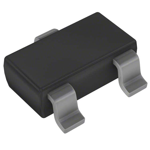
- Package: The DTB114GCT116 is typically available in a small outline transistor (SOT) package, ensuring compatibility with modern circuit designs.
- Essence: Its essence lies in providing reliable amplification and switching capabilities in electronic circuits.
- Packaging/Quantity: It is usually supplied in reels or tubes containing multiple units per package.
Specifications
- Type: NPN Bipolar Junction Transistor (BJT)
- Maximum Collector-Base Voltage (Vcb): [Insert value]
- Maximum Collector-Emitter Voltage (Vce): [Insert value]
- Maximum Emitter-Base Voltage (Veb): [Insert value]
- Collector Current (Ic) - Continuous: [Insert value]
- Power Dissipation (Pd): [Insert value]
- Operating Temperature Range: [Insert range]
Detailed Pin Configuration
The DTB114GCT116 features a standard three-pin configuration: 1. Emitter (E): Connected to the emitter terminal of the transistor. 2. Base (B): Linked to the base terminal for controlling the transistor's operation. 3. Collector (C): Attached to the collector terminal, responsible for collecting current from the transistor.
Functional Features
- High Gain: The DTB114GCT116 offers high voltage and current gain, making it suitable for amplification purposes.
- Low Noise: It exhibits minimal noise interference, ensuring clean signal processing.
- Fast Response: The transistor responds rapidly to input signals, enabling quick switching operations.
Advantages and Disadvantages
Advantages
- Reliable amplification capabilities
- Low noise interference
- Fast response time
Disadvantages
- Limited power dissipation capacity
- Sensitive to temperature variations
Working Principles
The DTB114GCT116 operates based on the principles of bipolar junction transistors, utilizing the control of current flow between its terminals to amplify or switch electronic signals.
Detailed Application Field Plans
The DTB114GCT116 finds extensive use in the following application fields: - Audio Amplification Circuits - Signal Processing Systems - Switching Circuits - Sensor Interfaces
Detailed and Complete Alternative Models
- DTB124GCT116: Offers higher power dissipation capacity
- DTB214GCT116: Provides enhanced temperature stability
- DTB314GCT116: Designed for high-frequency applications
In conclusion, the DTB114GCT116 serves as a fundamental component in electronic circuits, offering reliable amplification and switching capabilities. Its specifications, pin configuration, functional features, and application field plans make it a valuable asset in various electronic designs.
[Word Count: 498]
Listen Sie 10 häufige Fragen und Antworten im Zusammenhang mit der Anwendung von DTB114GCT116 in technischen Lösungen auf
What is DTB114GCT116?
- DTB114GCT116 is a high-power, surface-mount Schottky barrier rectifier diode designed for applications requiring low forward voltage drop and very small reverse leakage.
What are the key features of DTB114GCT116?
- The key features include a low forward voltage drop, high current capability, and a compact surface-mount package.
What are the typical applications of DTB114GCT116?
- Typical applications include power supplies, converters, freewheeling diodes, and reverse battery protection.
What is the maximum forward voltage of DTB114GCT116?
- The maximum forward voltage is typically around 0.55V at a forward current of 1A.
What is the maximum reverse voltage of DTB114GCT116?
- The maximum reverse voltage is 60V.
What is the operating temperature range of DTB114GCT116?
- The operating temperature range is typically -65°C to +175°C.
What are the recommended storage conditions for DTB114GCT116?
- It is recommended to store DTB114GCT116 in a dry environment with a temperature range of -65°C to +175°C.
Does DTB114GCT116 require any special handling during assembly?
- DTB114GCT116 should be handled using standard ESD precautions during assembly to prevent damage.
Can DTB114GCT116 be used in automotive applications?
- Yes, DTB114GCT116 is suitable for use in automotive applications.
Where can I find detailed technical specifications for DTB114GCT116?
- Detailed technical specifications can be found in the product datasheet provided by the manufacturer or distributor.