

Siehe Spezifikationen für Produktdetails.
SMMBFJ309LT1G
Product Overview
Category
The SMMBFJ309LT1G belongs to the category of field-effect transistors (FETs).
Use
It is commonly used as a switching device in electronic circuits.
Characteristics
- Low threshold voltage
- Small package size
- High switching speed
- Low input capacitance
Package
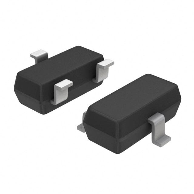
The SMMBFJ309LT1G is typically available in a small surface-mount package.
Essence
This FET is essential for controlling the flow of current in electronic devices.
Packaging/Quantity
It is usually packaged in reels containing a specific quantity, such as 3000 units per reel.
Specifications
- Drain-Source Voltage: 20V
- Continuous Drain Current: 100mA
- Total Power Dissipation: 225mW
- Operating Temperature Range: -55°C to 150°C
Detailed Pin Configuration
The SMMBFJ309LT1G has three pins: 1. Source (S) 2. Gate (G) 3. Drain (D)
Functional Features
- Low threshold voltage allows for efficient control of the FET.
- High switching speed enables rapid on/off transitions.
- Small package size saves space in circuit designs.
Advantages and Disadvantages
Advantages
- Low threshold voltage enhances energy efficiency.
- High switching speed improves overall circuit performance.
- Small package size facilitates compact designs.
Disadvantages
- Limited maximum drain-source voltage compared to other FETs.
- Lower continuous drain current compared to some alternatives.
Working Principles
The SMMBFJ309LT1G operates based on the principle of field-effect modulation, where the voltage applied to the gate terminal controls the conductivity between the source and drain terminals.
Detailed Application Field Plans
The SMMBFJ309LT1G is widely used in applications such as: - Portable electronic devices - Battery management systems - Switching power supplies - LED lighting control circuits
Detailed and Complete Alternative Models
Some alternative models to the SMMBFJ309LT1G include: - SMMBFJ310LT1G - SMMBFJ308LT1G - SMMBFJ307LT1G
In conclusion, the SMMBFJ309LT1G is a versatile field-effect transistor with low threshold voltage, high switching speed, and compact packaging, making it suitable for various electronic applications.
[Word count: 313]
Listen Sie 10 häufige Fragen und Antworten im Zusammenhang mit der Anwendung von SMMBFJ309LT1G in technischen Lösungen auf
What is SMMBFJ309LT1G?
- SMMBFJ309LT1G is a small signal N-channel JFET transistor designed for high-speed switching applications.
What are the key features of SMMBFJ309LT1G?
- The key features include low on-state resistance, high forward transfer admittance, and low input capacitance.
What are the typical applications of SMMBFJ309LT1G?
- Typical applications include analog switches, choppers, and high-speed pulse circuits.
What is the maximum drain-source voltage for SMMBFJ309LT1G?
- The maximum drain-source voltage is 25V.
What is the maximum continuous drain current for SMMBFJ309LT1G?
- The maximum continuous drain current is 50mA.
What is the operating temperature range for SMMBFJ309LT1G?
- The operating temperature range is -55°C to 150°C.
What is the package type for SMMBFJ309LT1G?
- The package type is SOT-23.
What are the recommended storage conditions for SMMBFJ309LT1G?
- It is recommended to store SMMBFJ309LT1G in a dry environment at temperatures between -65°C and 150°C.
What are the typical input and output capacitances for SMMBFJ309LT1G?
- The typical input capacitance is 2pF, and the typical output capacitance is 1.5pF.
What are the equivalent circuit parameters for SMMBFJ309LT1G?
- The equivalent circuit parameters include gate-source cutoff voltage, forward transfer admittance, and input capacitance.