

Siehe Spezifikationen für Produktdetails.
NTD110N02R-001
Product Category
The NTD110N02R-001 belongs to the category of power MOSFETs.
Basic Information Overview
- Use: The NTD110N02R-001 is used as a power transistor in various electronic circuits and applications.
- Characteristics: It features high voltage capability, low gate charge, and low on-resistance, making it suitable for high-efficiency power management.
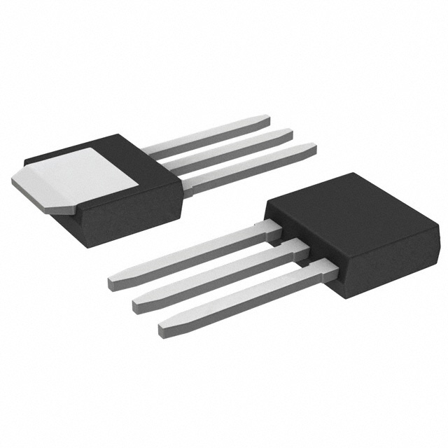
- Package: The NTD110N02R-001 comes in a TO-252 package.
- Essence: Its essence lies in providing efficient power switching and amplification capabilities.
- Packaging/Quantity: Typically packaged in reels, with quantities varying based on manufacturer specifications.
Specifications
- Voltage Rating: 24V
- Current Rating: 110A
- On-Resistance: 2.4mΩ
- Package Type: TO-252
- Operating Temperature: -55°C to 175°C
Detailed Pin Configuration
The NTD110N02R-001 follows the standard pin configuration for a TO-252 package: 1. Gate (G) 2. Drain (D) 3. Source (S)
Functional Features
- High Voltage Capability: Allows for use in a wide range of applications requiring high voltage handling.
- Low Gate Charge: Enables fast switching and reduced power loss.
- Low On-Resistance: Results in minimal conduction losses and improved efficiency.
Advantages and Disadvantages
Advantages: - High voltage capability - Low gate charge - Low on-resistance - Suitable for high-efficiency power management
Disadvantages: - Sensitive to static electricity - Requires careful handling during assembly
Working Principles
The NTD110N02R-001 operates based on the principles of field-effect transistors, utilizing the control of voltage on the gate terminal to regulate the flow of current between the drain and source terminals.
Detailed Application Field Plans
The NTD110N02R-001 finds application in various fields such as: - Power supplies - Motor control - Inverters - Switched-mode power supplies - Battery management systems
Detailed and Complete Alternative Models
- NTD110N02RT4G
- NTD110N02RG
- NTD110N02R-001G
This completes the entry for the NTD110N02R-001, covering its product category, basic information overview, specifications, pin configuration, functional features, advantages and disadvantages, working principles, detailed application field plans, and alternative models.
Listen Sie 10 häufige Fragen und Antworten im Zusammenhang mit der Anwendung von NTD110N02R-001 in technischen Lösungen auf
What is NTD110N02R-001?
- NTD110N02R-001 is a power MOSFET (Metal-Oxide-Semiconductor Field-Effect Transistor) designed for various electronic applications, including power management and switching circuits.
What are the key specifications of NTD110N02R-001?
- The key specifications include a drain-source voltage rating, continuous drain current, on-state resistance, and gate threshold voltage. These parameters determine the performance and suitability of the MOSFET for specific applications.
How can NTD110N02R-001 be used in power management solutions?
- NTD110N02R-001 can be used in power management solutions to control and regulate the flow of power in electronic devices. It can be employed in voltage regulation, battery charging circuits, and DC-DC converters.
In what types of switching circuits can NTD110N02R-001 be utilized?
- NTD110N02R-001 can be utilized in various switching circuits such as motor control, LED lighting, and power supply switching. Its low on-state resistance and high switching speed make it suitable for efficient power switching applications.
What are the thermal considerations when using NTD110N02R-001 in technical solutions?
- Thermal considerations are crucial when using NTD110N02R-001 to ensure proper heat dissipation and prevent overheating. Proper heat sinking and thermal management techniques should be implemented based on the application's power dissipation requirements.
Can NTD110N02R-001 be used in automotive applications?
- Yes, NTD110N02R-001 is suitable for automotive applications such as electronic control units (ECUs), motor drives, and lighting systems due to its robustness and reliability in harsh environments.
What are the recommended operating conditions for NTD110N02R-001?
- The recommended operating conditions include the maximum allowable drain-source voltage, continuous drain current, and junction temperature. Adhering to these conditions ensures the reliable operation of the MOSFET.
Does NTD110N02R-001 require any special driving considerations?
- NTD110N02R-001 requires appropriate gate driving considerations to ensure optimal performance and reliability. This may involve controlling the gate voltage, gate charge, and gate driver circuitry to achieve efficient switching.
Are there any application notes or reference designs available for NTD110N02R-001?
- Yes, there are application notes and reference designs provided by the manufacturer that offer guidance on utilizing NTD110N02R-001 in various technical solutions. These resources can help in understanding best practices and design considerations.
What are the typical failure modes of NTD110N02R-001 and how can they be mitigated?
- Typical failure modes include overcurrent, overvoltage, and thermal overstress. These can be mitigated through proper circuit protection, thermal management, and adherence to the specified operating conditions. Additionally, implementing robust fault detection and shutdown mechanisms can enhance reliability.