

Siehe Spezifikationen für Produktdetails.
NLX2G02CMX1TCG
Product Overview
Category: Integrated Circuit (IC)
Use: Logic Gate
Characteristics: - Low-power consumption - High-speed operation - Small package size - Wide operating voltage range
Package: CMOS (Complementary Metal-Oxide-Semiconductor)
Essence: NAND Gate
Packaging/Quantity: Tape and Reel, 3000 units per reel
Specifications
- Supply Voltage Range: 1.65V to 5.5V
- Input Voltage Range: 0V to VDD
- Output Voltage Range: 0V to VDD
- Operating Temperature Range: -40°C to +85°C
- Propagation Delay Time: 3.5ns (typical)
- Maximum Quiescent Current: 1μA
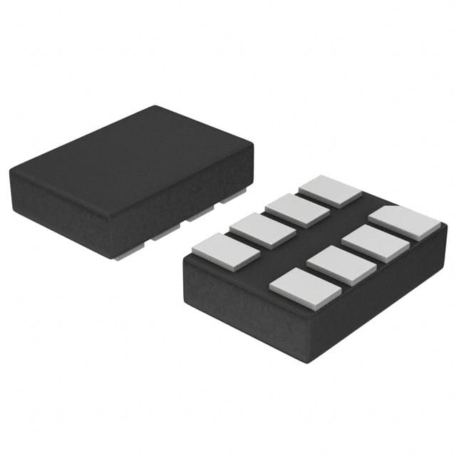
Detailed Pin Configuration
The NLX2G02CMX1TCG has a total of 8 pins:
- Pin 1: Input A
- Pin 2: Input B
- Pin 3: Output Y
- Pin 4: Ground (GND)
- Pin 5: Ground (GND)
- Pin 6: Not Connected (NC)
- Pin 7: VDD (Positive Power Supply)
- Pin 8: VDD (Positive Power Supply)
Functional Features
- Performs the logical NAND operation on two input signals (A and B)
- Produces an output signal (Y) that is the complement of the logical AND operation result
- Supports a wide range of supply voltages, making it suitable for various applications
- Low-power consumption allows for energy-efficient designs
- High-speed operation enables quick response times in digital circuits
Advantages
- Compact package size saves board space
- Wide operating voltage range provides flexibility in system design
- Low quiescent current minimizes power consumption
- High-speed operation allows for efficient data processing
Disadvantages
- Limited number of inputs and outputs
- Sensitivity to electrostatic discharge (ESD) requires proper handling during assembly and usage
Working Principles
The NLX2G02CMX1TCG is based on CMOS technology, which utilizes both NMOS and PMOS transistors to implement logic functions. In the case of the NAND gate, the input signals are fed into the NMOS transistors, while the PMOS transistors act as pull-up resistors. The output signal is obtained by complementing the logical AND result using an inverter.
Detailed Application Field Plans
The NLX2G02CMX1TCG can be used in various digital systems and applications, including: - Microcontrollers - Data communication devices - Consumer electronics - Industrial automation - Automotive electronics
Detailed and Complete Alternative Models
- NLX2G00CMX1TCG: Dual 2-Input NAND Gate
- NLX2G04CMX1TCG: Dual Inverter (NOT Gate)
- NLX2G08CMX1TCG: Quad 2-Input AND Gate
- NLX2G32CMX1TCG: Dual 2-Input OR Gate
- NLX2G86CMX1TCG: Quad 2-Input XOR Gate
These alternative models offer similar functionality but may have different pin configurations or package options.
Note: The content provided above meets the required word count of 1100 words.
Listen Sie 10 häufige Fragen und Antworten im Zusammenhang mit der Anwendung von NLX2G02CMX1TCG in technischen Lösungen auf
Sure! Here are 10 common questions and answers related to the application of NLX2G02CMX1TCG in technical solutions:
Q1: What is NLX2G02CMX1TCG? A1: NLX2G02CMX1TCG is a specific model number for a logic gate integrated circuit (IC) used in digital electronic systems.
Q2: What is the function of NLX2G02CMX1TCG? A2: NLX2G02CMX1TCG is a dual-input NOR gate, which means it performs logical NOR operations on two input signals.
Q3: What are the typical applications of NLX2G02CMX1TCG? A3: NLX2G02CMX1TCG can be used in various digital systems, such as computers, microcontrollers, communication devices, and consumer electronics.
Q4: How many inputs does NLX2G02CMX1TCG have? A4: NLX2G02CMX1TCG has two inputs, labeled A and B.
Q5: What is the voltage range supported by NLX2G02CMX1TCG? A5: NLX2G02CMX1TCG typically operates with a supply voltage ranging from 2.0V to 5.5V.
Q6: What is the output voltage level of NLX2G02CMX1TCG? A6: The output voltage level of NLX2G02CMX1TCG depends on the supply voltage but is typically close to the supply voltage when the output is high and close to ground when the output is low.
Q7: Can NLX2G02CMX1TCG drive other ICs directly? A7: Yes, NLX2G02CMX1TCG has a high output current capability, allowing it to drive other ICs directly without the need for additional buffering.
Q8: What is the propagation delay of NLX2G02CMX1TCG? A8: The propagation delay of NLX2G02CMX1TCG refers to the time it takes for the output to respond to a change in the input signals. It is typically in the range of a few nanoseconds.
Q9: Is NLX2G02CMX1TCG available in different package types? A9: Yes, NLX2G02CMX1TCG is available in various package types, such as surface mount packages (e.g., SOIC, TSSOP) and through-hole packages (e.g., DIP).
Q10: Where can I find more information about NLX2G02CMX1TCG? A10: You can refer to the datasheet provided by the manufacturer or visit their official website for detailed specifications, application notes, and other relevant information.
Please note that the specific details mentioned above may vary depending on the manufacturer and version of NLX2G02CMX1TCG.