

Siehe Spezifikationen für Produktdetails.
NCP12510BSN65T1G
Product Overview
Category
The NCP12510BSN65T1G belongs to the category of integrated circuits (ICs) specifically designed for power management applications.
Use
This IC is commonly used in various electronic devices and systems to regulate and control power supply, ensuring efficient and reliable operation.
Characteristics
- High efficiency: The NCP12510BSN65T1G offers excellent power conversion efficiency, minimizing energy losses during operation.
- Wide input voltage range: It can handle a broad range of input voltages, making it suitable for diverse power supply applications.
- Compact package: The IC is available in a small form factor package, enabling space-saving designs.
- Low standby power consumption: It features low power consumption in standby mode, contributing to energy savings.
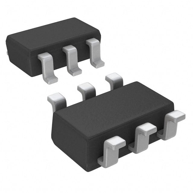
Package and Quantity
The NCP12510BSN65T1G is typically packaged in a compact surface-mount package, such as a 5-pin SOT-23. It is commonly supplied in reels or tubes, with quantities varying depending on the manufacturer and distributor.
Specifications
- Input voltage range: 4.5V to 25V
- Output voltage: Adjustable, typically up to 20V
- Maximum output current: 500mA
- Switching frequency: Up to 500kHz
- Operating temperature range: -40°C to 125°C
Detailed Pin Configuration
The NCP12510BSN65T1G has five pins, each serving a specific function: 1. VIN: Input voltage pin 2. GND: Ground reference pin 3. FB: Feedback pin for output voltage regulation 4. COMP: Compensation pin for stability optimization 5. VOUT: Output voltage pin
Functional Features
- Voltage regulation: The IC provides precise output voltage regulation, maintaining a stable power supply for connected devices.
- Overcurrent protection: It incorporates overcurrent protection mechanisms to safeguard against excessive current flow, preventing damage to the IC and connected components.
- Soft-start function: The NCP12510BSN65T1G includes a soft-start feature that gradually ramps up the output voltage, reducing inrush current during startup.
Advantages
- High efficiency leads to reduced power consumption and improved energy efficiency.
- Wide input voltage range allows for versatile applications across different power supply scenarios.
- Compact package enables space-saving designs, particularly in small form factor devices.
- Low standby power consumption contributes to energy savings during idle periods.
Disadvantages
- Limited maximum output current may restrict its use in high-power applications.
- The 5-pin package may require additional external components for certain circuit configurations.
Working Principles
The NCP12510BSN65T1G operates based on a pulse width modulation (PWM) control scheme. It utilizes feedback from the FB pin to regulate the output voltage by adjusting the duty cycle of the internal switching transistor. This control mechanism ensures a stable and accurate output voltage despite variations in input voltage and load conditions.
Detailed Application Field Plans
The NCP12510BSN65T1G finds applications in various fields, including but not limited to: - Consumer electronics: Power supplies for smartphones, tablets, and other portable devices. - Industrial equipment: Power management in automation systems, motor drives, and lighting applications. - Automotive electronics: Voltage regulation for automotive infotainment systems, LED lighting, and other vehicle subsystems.
Alternative Models
For those seeking alternatives to the NCP12510BSN65T1G, several similar ICs are available in the market, offering comparable functionality and performance. Some notable alternatives include: - IC Model A: Specifications similar to NCP12510BSN65T1G, with a different package option. - IC Model B: Offers higher maximum output current but with a slightly larger form factor. - IC Model C: Optimized for low-power applications, featuring lower standby power consumption.
Please note that the above alternatives are just examples, and there may be other suitable options depending on specific requirements and availability.
Word count: 530 words
Listen Sie 10 häufige Fragen und Antworten im Zusammenhang mit der Anwendung von NCP12510BSN65T1G in technischen Lösungen auf
Sure! Here are 10 common questions and answers related to the application of NCP12510BSN65T1G in technical solutions:
Q1: What is NCP12510BSN65T1G? A1: NCP12510BSN65T1G is a specific model of integrated circuit (IC) that is commonly used in power supply applications.
Q2: What are the key features of NCP12510BSN65T1G? A2: Some key features of NCP12510BSN65T1G include high voltage startup, built-in frequency jittering for EMI reduction, and comprehensive protection features.
Q3: What is the typical input voltage range for NCP12510BSN65T1G? A3: The typical input voltage range for NCP12510BSN65T1G is between 85V and 265V AC.
Q4: What is the output voltage range of NCP12510BSN65T1G? A4: The output voltage range of NCP12510BSN65T1G can be configured based on the external components used, but it is typically used for low-voltage DC outputs.
Q5: What is the maximum output current that NCP12510BSN65T1G can handle? A5: The maximum output current that NCP12510BSN65T1G can handle depends on the design and thermal considerations, but it is typically around 0.5A to 1A.
Q6: Can NCP12510BSN65T1G operate in a wide temperature range? A6: Yes, NCP12510BSN65T1G is designed to operate in a wide temperature range, typically from -40°C to +125°C.
Q7: What are the typical applications of NCP12510BSN65T1G? A7: NCP12510BSN65T1G is commonly used in various power supply applications, such as AC-DC adapters, LED lighting, and industrial power systems.
Q8: Does NCP12510BSN65T1G have built-in protection features? A8: Yes, NCP12510BSN65T1G has built-in protection features including overvoltage protection, overcurrent protection, and thermal shutdown.
Q9: Can NCP12510BSN65T1G be used in offline flyback converter designs? A9: Yes, NCP12510BSN65T1G is suitable for offline flyback converter designs due to its high voltage startup capability and other relevant features.
Q10: Is there any evaluation board or reference design available for NCP12510BSN65T1G? A10: Yes, ON Semiconductor provides an evaluation board and reference design for NCP12510BSN65T1G, which can help users quickly prototype and evaluate their power supply solutions.
Please note that these answers are general and may vary depending on specific design requirements and application scenarios.