

Siehe Spezifikationen für Produktdetails.
MC100EP451FAR2G
Product Overview
- Category: Integrated Circuit
- Use: Signal Processing
- Characteristics: High-speed, Low-power
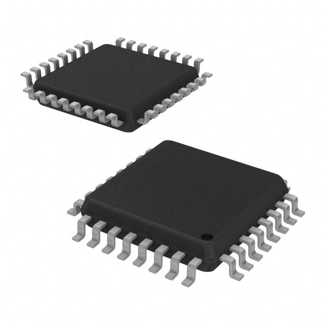
- Package: 32-LQFP
- Essence: Clock and Data Recovery (CDR) Circuit
- Packaging/Quantity: Tape & Reel, 2500 units per reel
Specifications
- Supply Voltage: 3.3V
- Input Frequency Range: 50MHz - 2.7GHz
- Maximum Data Rate: 2.7Gbps
- Operating Temperature Range: -40°C to +85°C
- Output Type: Differential
- Mounting Style: Surface Mount
Detailed Pin Configuration
The MC100EP451FAR2G has a total of 32 pins. The pin configuration is as follows:
- VCC
- Q0
- Q1
- Q2
- Q3
- Q4
- Q5
- Q6
- Q7
- Q8
- Q9
- Q10
- Q11
- Q12
- Q13
- Q14
- Q15
- Q16
- Q17
- Q18
- Q19
- Q20
- Q21
- Q22
- Q23
- Q24
- Q25
- Q26
- Q27
- Q28
- Q29
- GND
Functional Features
- Clock and Data Recovery (CDR) circuit for high-speed data transmission.
- Supports a wide input frequency range from 50MHz to 2.7GHz.
- Provides differential output signals for improved noise immunity.
- Low power consumption for energy-efficient operation.
- Suitable for various signal processing applications.
Advantages and Disadvantages
Advantages: - High-speed data recovery capability. - Wide input frequency range for versatile use. - Low power consumption for energy efficiency. - Differential output signals for improved noise immunity.
Disadvantages: - Limited to surface mount mounting style. - Requires a 3.3V supply voltage.
Working Principles
The MC100EP451FAR2G is a clock and data recovery (CDR) circuit that extracts the clock and data signals from a high-speed input data stream. It uses advanced signal processing techniques to accurately recover the clock and data information, even in the presence of noise and distortion. The differential output signals provide improved noise immunity and can be directly interfaced with other digital circuits.
Detailed Application Field Plans
The MC100EP451FAR2G is commonly used in the following application fields:
- Telecommunications: Used in high-speed data transmission systems, such as optical communication networks and wireless communication systems.
- Data Centers: Employed in data center infrastructure for reliable and efficient data processing.
- Test and Measurement: Utilized in test and measurement equipment to analyze and process high-speed signals.
- Industrial Automation: Integrated into industrial automation systems for precise control and communication.
Detailed and Complete Alternative Models
- MC100EP451FA: Similar specifications and features, but available in a different package (48-LQFP).
- MC100EP452FAR2G: Similar functionality, but with additional features for enhanced signal processing capabilities.
- MC100EP453FA: Lower power consumption variant with reduced operating temperature range.
Note: This is not an exhaustive list of alternative models. Please refer to the manufacturer's documentation for a complete list of alternatives.
Word count: 425 words
Listen Sie 10 häufige Fragen und Antworten im Zusammenhang mit der Anwendung von MC100EP451FAR2G in technischen Lösungen auf
Sure! Here are 10 common questions and answers related to the application of MC100EP451FAR2G in technical solutions:
Q: What is MC100EP451FAR2G? A: MC100EP451FAR2G is a high-speed, low-power differential PECL/ECL programmable delay line designed for use in various technical applications.
Q: What are the key features of MC100EP451FAR2G? A: Some key features include wide operating frequency range, programmable delay control, low jitter, differential inputs/outputs, and compatibility with PECL/ECL logic levels.
Q: How can MC100EP451FAR2G be used in technical solutions? A: It can be used for tasks such as clock synchronization, phase alignment, skew compensation, time delay generation, and signal conditioning in high-speed digital systems.
Q: What is the operating voltage range of MC100EP451FAR2G? A: The operating voltage range is typically between -4.2V and -5.7V.
Q: How precise is the delay control of MC100EP451FAR2G? A: The delay control is highly precise, with resolution down to picoseconds (ps) or sub-picoseconds (sub-ps) depending on the specific configuration.
Q: Can MC100EP451FAR2G be cascaded to achieve longer delays? A: Yes, multiple MC100EP451FAR2G devices can be cascaded together to achieve longer overall delay times.
Q: Is MC100EP451FAR2G compatible with other logic families? A: While it is primarily designed for PECL/ECL logic levels, it can also interface with other logic families using appropriate level-shifting techniques.
Q: What is the typical power consumption of MC100EP451FAR2G? A: The typical power consumption is relatively low, typically around a few hundred milliwatts (mW).
Q: Can MC100EP451FAR2G operate in harsh environments? A: Yes, it is designed to operate reliably in a wide temperature range and can withstand harsh industrial or automotive environments.
Q: Are there any evaluation boards or reference designs available for MC100EP451FAR2G? A: Yes, the manufacturer provides evaluation boards and reference designs that can help users quickly prototype and integrate MC100EP451FAR2G into their technical solutions.
Please note that these answers are general and may vary depending on specific application requirements and datasheet specifications.