

Siehe Spezifikationen für Produktdetails.
FST3384MTCX
Product Overview
Category
FST3384MTCX belongs to the category of integrated circuits (ICs).
Use
This product is commonly used in electronic devices for signal transmission and amplification.
Characteristics
- FST3384MTCX is a high-speed, low-power quad buffer with 3-state outputs.
- It operates at a voltage range of 2.0V to 5.5V, making it suitable for various applications.
- The device offers a high-speed propagation delay of only a few nanoseconds.
- It has a low input and output capacitance, reducing power consumption and improving performance.
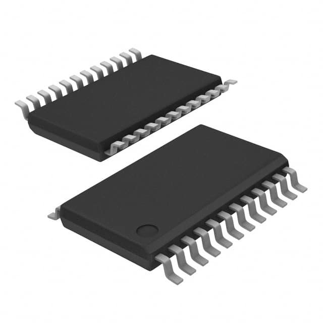
Package
FST3384MTCX is available in a small outline package (SOIC) with 14 pins.
Essence
The essence of FST3384MTCX lies in its ability to provide efficient signal buffering and amplification while consuming minimal power.
Packaging/Quantity
This product is typically packaged in reels or tubes, containing a quantity of 250 units per package.
Specifications
- Supply Voltage: 2.0V - 5.5V
- Input Voltage Range: GND to VCC
- Output Voltage Range: GND to VCC
- Operating Temperature Range: -40°C to +85°C
- Input Capacitance: 3pF (typical)
- Output Capacitance: 6pF (typical)
- Propagation Delay: 2.5ns (typical)
Detailed Pin Configuration
- A1 - Input A
- Y1 - Output A
- GND - Ground
- Y2 - Output B
- A2 - Input B
- Y3 - Output C
- A3 - Input C
- VCC - Power Supply
- Y4 - Output D
- A4 - Input D
- OE - Output Enable
- GND - Ground
- NC - No Connection
- VCC - Power Supply
Functional Features
- FST3384MTCX provides 3-state outputs, allowing multiple devices to share a common bus without interference.
- It offers high-speed signal transmission and amplification, making it suitable for applications requiring fast data transfer.
- The device has a low power consumption, contributing to energy-efficient designs.
- It exhibits excellent noise immunity, ensuring reliable signal integrity.
Advantages and Disadvantages
Advantages
- High-speed operation
- Low power consumption
- 3-state outputs for bus sharing
- Excellent noise immunity
Disadvantages
- Limited voltage range (2.0V - 5.5V)
- Relatively small package size
Working Principles
FST3384MTCX operates as a buffer by receiving input signals and amplifying them to drive the output pins. The 3-state outputs allow the device to be enabled or disabled, enabling multiple devices to share a common bus without causing conflicts. The low power consumption and high-speed operation are achieved through efficient circuit design and optimized semiconductor materials.
Detailed Application Field Plans
FST3384MTCX finds applications in various electronic systems, including but not limited to: - Data communication equipment - Computer peripherals - Industrial automation - Automotive electronics - Consumer electronics
Detailed and Complete Alternative Models
- SN74LVC244A: Octal buffer/line driver with 3-state outputs
- MC74VHC244: Octal buffer/line driver with 3-state outputs
- CD74HCT125: Quad buffer/line driver with 3-state outputs
- 74HC125: Quad buffer/line driver with 3-state outputs
- SN74LVTH244A: Octal buffer/line driver with 3-state outputs
These alternative models offer similar functionality and can be considered as substitutes for FST3384MTCX in various applications.
Word count: 497 words
Listen Sie 10 häufige Fragen und Antworten im Zusammenhang mit der Anwendung von FST3384MTCX in technischen Lösungen auf
Sure! Here are 10 common questions and answers related to the application of FST3384MTCX in technical solutions:
Q: What is FST3384MTCX? A: FST3384MTCX is a specific model of a high-speed, low-power quad bilateral switch used in various technical applications.
Q: What are the key features of FST3384MTCX? A: The key features of FST3384MTCX include low ON resistance, wide voltage range, high bandwidth, low power consumption, and compatibility with different logic families.
Q: In which technical solutions can FST3384MTCX be used? A: FST3384MTCX can be used in applications such as analog signal switching, audio/video routing, data acquisition systems, test equipment, and communication systems.
Q: What is the maximum voltage rating for FST3384MTCX? A: The maximum voltage rating for FST3384MTCX is typically around 5V or 3.3V, depending on the specific variant.
Q: How many channels does FST3384MTCX have? A: FST3384MTCX has four independent channels, allowing for simultaneous switching of multiple signals.
Q: What is the typical ON resistance of FST3384MTCX? A: The typical ON resistance of FST3384MTCX is very low, usually in the range of a few ohms.
Q: Can FST3384MTCX handle both analog and digital signals? A: Yes, FST3384MTCX is designed to handle both analog and digital signals effectively.
Q: Is FST3384MTCX compatible with different logic families? A: Yes, FST3384MTCX is compatible with various logic families such as TTL, CMOS, and LVCMOS.
Q: What is the operating temperature range for FST3384MTCX? A: The operating temperature range for FST3384MTCX typically spans from -40°C to +85°C.
Q: Are there any specific precautions to consider when using FST3384MTCX? A: It is recommended to follow the manufacturer's datasheet and guidelines for proper handling, voltage levels, and ESD protection during the application of FST3384MTCX.
Please note that the answers provided here are general and may vary depending on the specific variant or manufacturer's specifications of FST3384MTCX.