

Siehe Spezifikationen für Produktdetails.
CD4514BCN
Product Overview
Category
CD4514BCN belongs to the category of integrated circuits (ICs).
Use
It is commonly used as a 4-bit latch/4-to-16 line decoder in various electronic applications.
Characteristics
- CD4514BCN is a CMOS-based IC.
- It operates at a wide voltage range, typically between 3V and 18V.
- The IC has a high noise immunity and low power consumption.
- It offers a high output current capability.
Package
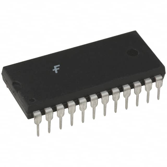
CD4514BCN is available in a 24-pin DIP (Dual Inline Package) format.
Essence
The essence of CD4514BCN lies in its ability to function as both a latch and a decoder, making it versatile for different circuit designs.
Packaging/Quantity
CD4514BCN is typically packaged in tubes or trays, with quantities varying based on customer requirements.
Specifications
- Supply Voltage: 3V - 18V
- Input Voltage: 0V - VDD
- Output Voltage: 0V - VDD
- Operating Temperature Range: -55°C to +125°C
- Maximum Power Dissipation: 500mW
Detailed Pin Configuration
- VSS (Ground)
- A0 (Address Input)
- A1 (Address Input)
- A2 (Address Input)
- A3 (Address Input)
- E1 (Enable Input)
- E2 (Enable Input)
- E3 (Enable Input)
- E4 (Enable Input)
- O0 (Output)
- O1 (Output)
- O2 (Output)
- O3 (Output)
- O4 (Output)
- O5 (Output)
- O6 (Output)
- O7 (Output)
- O8 (Output)
- O9 (Output)
- O10 (Output)
- O11 (Output)
- O12 (Output)
- O13 (Output)
- VDD (Supply Voltage)
Functional Features
- CD4514BCN acts as a 4-bit latch, allowing data to be stored temporarily.
- It also functions as a 4-to-16 line decoder, converting the input address into an output signal.
- The IC offers a high level of noise immunity, ensuring reliable operation in noisy environments.
- It has a wide operating voltage range, making it compatible with various power supply configurations.
Advantages and Disadvantages
Advantages
- Versatile functionality as both a latch and a decoder.
- Wide operating voltage range.
- High noise immunity.
- Low power consumption.
Disadvantages
- Limited number of output lines (16).
- Requires external components for complete circuit implementation.
Working Principles
CD4514BCN operates by latching the input data when the enable inputs (E1-E4) are active. The address inputs (A0-A3) determine which latch is enabled. The selected latch's output is then decoded to activate the corresponding output line. The IC uses CMOS technology, providing low power consumption and high noise immunity.
Detailed Application Field Plans
CD4514BCN finds applications in various fields, including: 1. Digital electronics 2. Communication systems 3. Industrial automation 4. Automotive electronics 5. Consumer electronics
Detailed and Complete Alternative Models
Some alternative models to CD4514BCN include: 1. CD4514BE: Similar functionality but available in a different package format (16-pin DIP). 2. CD4514BNSR: Surface mount version of CD4514BCN. 3. CD4514BM96: Tape and reel packaging for automated assembly.
These alternative models offer similar functionality but may vary in package type, pin configuration, or packaging options.
Word count: 536 words
Listen Sie 10 häufige Fragen und Antworten im Zusammenhang mit der Anwendung von CD4514BCN in technischen Lösungen auf
Sure! Here are 10 common questions and answers related to the application of CD4514BCN in technical solutions:
Q: What is CD4514BCN? A: CD4514BCN is a 4-bit latch/4-to-16 line decoder IC (integrated circuit) commonly used in digital electronics.
Q: What is the purpose of CD4514BCN? A: CD4514BCN is used to decode a 4-bit binary input into one of 16 possible output lines, making it useful for addressing multiple devices or selecting different functions.
Q: How does CD4514BCN work? A: CD4514BCN works by taking a 4-bit binary input and activating the corresponding output line based on the input value. It uses internal logic gates to perform the decoding operation.
Q: What voltage levels does CD4514BCN support? A: CD4514BCN typically operates at a supply voltage range of 3V to 18V, making it compatible with a wide range of digital systems.
Q: Can CD4514BCN be cascaded to increase the number of output lines? A: Yes, CD4514BCN can be cascaded by connecting the outputs of one IC to the inputs of another, allowing for expansion of the number of output lines.
Q: What is the maximum frequency at which CD4514BCN can operate? A: CD4514BCN has a maximum operating frequency of around 5 MHz, which means it can handle relatively high-speed digital signals.
Q: Are there any special considerations when using CD4514BCN in noisy environments? A: Yes, CD4514BCN is susceptible to noise interference, so it is recommended to use proper decoupling capacitors and ensure good grounding practices to minimize noise-related issues.
Q: Can CD4514BCN be used in both digital and analog applications? A: No, CD4514BCN is primarily designed for digital applications and may not provide accurate results when used in analog circuits.
Q: What are some common applications of CD4514BCN? A: CD4514BCN is commonly used in address decoding, data multiplexing, LED matrix control, keypad scanning, and other similar applications.
Q: Where can I find more information about CD4514BCN and its application examples? A: You can refer to the CD4514BCN datasheet provided by the manufacturer or search online for application notes and tutorials that demonstrate the usage of CD4514BCN in various technical solutions.
Please note that the answers provided here are general and may vary depending on specific requirements and use cases.