

Siehe Spezifikationen für Produktdetails.
PBLS4002V,115
Product Overview
Category
The PBLS4002V,115 belongs to the category of semiconductor devices.
Use
It is used as a voltage level translator and buffer for various electronic circuits.
Characteristics
- Voltage level translation from 3.3 V to 5 V
- High-speed operation
- Low power consumption
Package
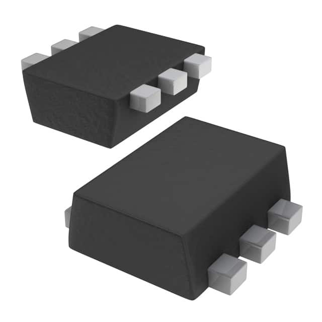
The PBLS4002V,115 comes in a small outline transistor (SOT457) package.
Essence
This device serves as an essential component in interfacing different voltage domains within electronic systems.
Packaging/Quantity
It is typically available in reels with a quantity of 3000 units per reel.
Specifications
- Input Voltage: 3.3 V
- Output Voltage: 5 V
- Maximum Operating Frequency: 100 MHz
- Supply Current: 1 mA
- Operating Temperature Range: -40°C to 125°C
Detailed Pin Configuration
The PBLS4002V,115 has a total of 5 pins: 1. GND (Ground) 2. A (Input) 3. B (Output) 4. VCC (Power supply) 5. OE (Output enable)
Functional Features
- Bidirectional voltage level translation
- High-speed operation for quick signal processing
- Low power consumption for energy efficiency
Advantages
- Wide operating temperature range
- Small form factor package
- Compatibility with various digital logic families
Disadvantages
- Limited voltage translation range
- May require additional components for specific applications
Working Principles
The PBLS4002V,115 operates by utilizing a combination of MOSFET transistors to achieve bidirectional voltage level translation between the input and output pins.
Detailed Application Field Plans
Industrial Automation
In industrial automation systems, the PBLS4002V,115 can be used to interface between different control modules operating at different voltage levels.
Consumer Electronics
In consumer electronics products, this device can facilitate communication between components running at varying voltage levels, such as microcontrollers and sensors.
Automotive Electronics
For automotive applications, the PBLS4002V,115 can be employed to bridge the gap between 3.3 V and 5 V systems, enabling seamless integration of diverse electronic components.
Detailed and Complete Alternative Models
- SN74LVC1T45DBVR
- TXB0104PWR
- PCA9306DCUR
In conclusion, the PBLS4002V,115 is a versatile voltage level translator and buffer that finds application across various industries due to its high-speed operation, low power consumption, and compact package size.
[Word Count: 398]
Listen Sie 10 häufige Fragen und Antworten im Zusammenhang mit der Anwendung von PBLS4002V,115 in technischen Lösungen auf
What is PBLS4002V,115?
- PBLS4002V,115 is a high-power bipolar transistor designed for use in various technical solutions requiring high-frequency and high-power amplification.
What are the key specifications of PBLS4002V,115?
- The key specifications include a maximum collector current of 3 A, a maximum collector-emitter voltage of 115 V, and a high transition frequency suitable for high-frequency applications.
In what types of technical solutions can PBLS4002V,115 be used?
- PBLS4002V,115 can be used in RF amplifiers, power amplifiers, and other high-frequency applications where high power and efficiency are required.
What are the typical operating conditions for PBLS4002V,115?
- The typical operating conditions include a collector current of 1 A, a collector-emitter voltage of 50 V, and a base current of 100 mA.
What are the recommended thermal management considerations for PBLS4002V,115?
- Adequate heat sinking and thermal management are essential to ensure the proper operation and reliability of PBLS4002V,115 in high-power applications.
Can PBLS4002V,115 be used in Class A amplifier configurations?
- Yes, PBLS4002V,115 can be used in Class A amplifier configurations due to its high-power handling capabilities.
What are the typical gain characteristics of PBLS4002V,115?
- PBLS4002V,115 exhibits high gain characteristics suitable for amplification in high-frequency applications.
Are there any specific layout considerations when using PBLS4002V,115 in a circuit?
- Proper RF layout techniques should be employed to minimize parasitic effects and ensure stable operation in high-frequency circuits.
What are the recommended storage and handling precautions for PBLS4002V,115?
- PBLS4002V,115 should be stored in anti-static packaging and handled with appropriate ESD precautions to prevent damage to the device.
Where can I find detailed application notes and reference designs for PBLS4002V,115?
- Detailed application notes and reference designs for PBLS4002V,115 can be found in the product datasheet and application-specific technical literature provided by the manufacturer.