

Siehe Spezifikationen für Produktdetails.
Encyclopedia Entry: 74LVC821ADB,112
Product Overview
- Category: Integrated Circuit (IC)
- Use: Logic Level Shifter
- Characteristics: High-speed, low-power, voltage level translation
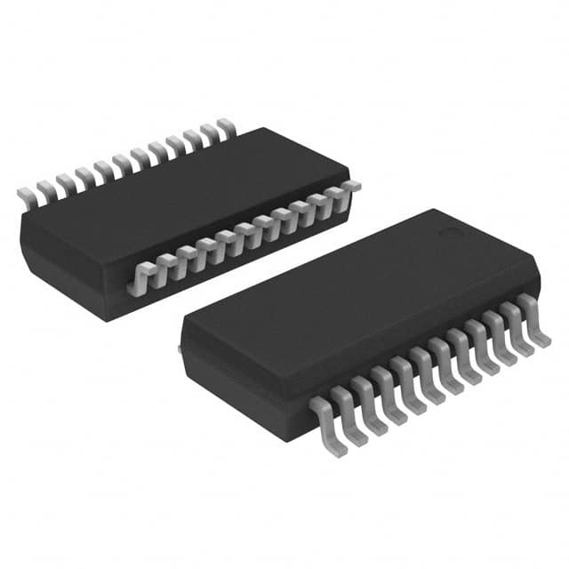
- Package: TSSOP-20
- Essence: Bi-directional voltage level translator
Packaging/Quantity
- Packaging: Tape and Reel
- Quantity: 2500 units per reel
Specifications
- Supply Voltage Range: 1.65V to 5.5V
- High-level Input Voltage (VIH): 2.3V to VCC + 0.3V
- Low-level Input Voltage (VIL): -0.3V to 0.8V
- High-level Output Voltage (VOH): VCC - 0.4V
- Low-level Output Voltage (VOL): 0.4V
- Maximum Operating Frequency: 100 MHz
Detailed Pin Configuration
The 74LVC821ADB,112 IC has a total of 20 pins. The pin configuration is as follows:
- A1
- B1
- GND
- B2
- A2
- OE#
- Y1
- Y2
- GND
- VCC
- A3
- B3
- GND
- B4
- A4
- OE#
- Y3
- Y4
- GND
- VCC
Functional Features
- Bi-directional voltage level shifting between two different voltage domains.
- Supports bidirectional data transfer with automatic direction sensing.
- Provides non-inverting level shifting for both high-to-low and low-to-high transitions.
- Allows interfacing between devices operating at different voltage levels.
Advantages
- High-speed operation allows for efficient data transfer.
- Low-power consumption makes it suitable for battery-powered applications.
- Wide supply voltage range enables compatibility with various systems.
- Bi-directional functionality simplifies circuit design and reduces component count.
Disadvantages
- Limited maximum operating frequency may not be suitable for high-speed applications.
- TSSOP-20 package may require careful handling during assembly.
Working Principles
The 74LVC821ADB,112 is a voltage level translator that operates by utilizing a combination of MOSFETs and CMOS technology. It provides bidirectional voltage translation between two different voltage domains, allowing seamless communication between devices operating at different voltage levels. The IC automatically senses the direction of data flow and performs non-inverting level shifting to ensure proper signal integrity.
Detailed Application Field Plans
The 74LVC821ADB,112 can be used in various applications where voltage level translation is required. Some potential application fields include: - Communication systems - Data acquisition systems - Industrial automation - Consumer electronics - Automotive electronics
Alternative Models
- SN74LVC821ADB,112
- MC74LVC821ADB,112
- CD74LVC821ADB,112
These alternative models offer similar functionality and can be used as substitutes for the 74LVC821ADB,112 in compatible applications.
In conclusion, the 74LVC821ADB,112 is a high-speed, low-power voltage level translator integrated circuit. Its bi-directional functionality, wide supply voltage range, and compact package make it suitable for various applications in different industries. However, its limited maximum operating frequency and specific package type should be considered when selecting this IC for a particular design.
Listen Sie 10 häufige Fragen und Antworten im Zusammenhang mit der Anwendung von 74LVC821ADB,112 in technischen Lösungen auf
Sure! Here are 10 common questions and answers related to the application of 74LVC821ADB,112 in technical solutions:
Q: What is the function of the 74LVC821ADB,112? A: The 74LVC821ADB,112 is a 10-bit buffer/driver with 3-state outputs.
Q: What is the voltage range supported by the 74LVC821ADB,112? A: The 74LVC821ADB,112 supports a voltage range of 1.65V to 5.5V.
Q: How many inputs does the 74LVC821ADB,112 have? A: The 74LVC821ADB,112 has 10 inputs.
Q: Can the 74LVC821ADB,112 be used for bidirectional communication? A: No, the 74LVC821ADB,112 is a unidirectional buffer/driver and does not support bidirectional communication.
Q: What is the maximum output current of the 74LVC821ADB,112? A: The 74LVC821ADB,112 can provide a maximum output current of 24mA.
Q: Does the 74LVC821ADB,112 have internal pull-up or pull-down resistors? A: No, the 74LVC821ADB,112 does not have internal pull-up or pull-down resistors.
Q: Can the 74LVC821ADB,112 be cascaded to drive more than 10 outputs? A: Yes, multiple 74LVC821ADB,112 chips can be cascaded to drive more than 10 outputs.
Q: Is the 74LVC821ADB,112 compatible with TTL logic levels? A: Yes, the 74LVC821ADB,112 is compatible with both TTL and CMOS logic levels.
Q: What is the power supply voltage required for the 74LVC821ADB,112? A: The 74LVC821ADB,112 requires a power supply voltage of 1.65V to 5.5V.
Q: Can the 74LVC821ADB,112 be used in high-speed applications? A: Yes, the 74LVC821ADB,112 is designed for high-speed operation and can be used in such applications.
Please note that these answers are general and may vary depending on the specific requirements and use cases. It's always recommended to refer to the datasheet and consult the manufacturer for detailed information.