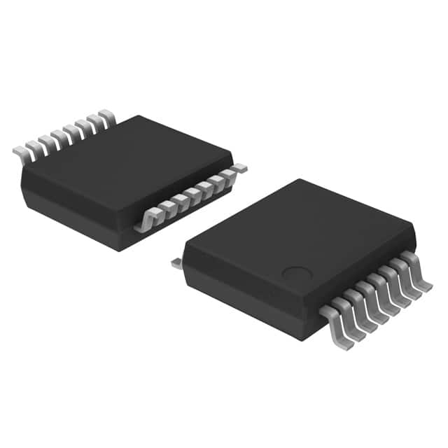
Siehe Spezifikationen für Produktdetails.

74LVC109DB,112
Basic Information Overview
- Category: Integrated Circuit (IC)
- Use: Flip-Flop
- Characteristics: Low-voltage CMOS dual D-type flip-flop with set and reset; operates at 1.65V to 5.5V voltage range
- Package: SSOP-16
- Essence: Dual D-type flip-flop with complementary outputs
- Packaging/Quantity: Tape and reel, 2500 units per reel
Specifications
- Supply Voltage Range: 1.65V to 5.5V
- High-Level Input Voltage: 0.7 x VCC
- Low-Level Input Voltage: 0.3 x VCC
- High-Level Output Voltage: 0.9 x VCC
- Low-Level Output Voltage: 0.1 x VCC
- Maximum Operating Frequency: 100 MHz
- Propagation Delay Time: 4.2 ns (typical)
Detailed Pin Configuration
The 74LVC109DB,112 IC has a total of 16 pins. The pin configuration is as follows:
+---+--+---+
   CLR |1  +--+ 16| VCC
   D1  |2       15| Q1
   D2  |3       14| Q2
   GND |4       13| Q3
   CP  |5       12| Q4
   PR  |6       11| Q5
   Q6  |7       10| Q6
   Q7  |8        9| Q7
        +---------+
Functional Features
- Dual D-type flip-flop with independent set and reset inputs
- Complementary outputs for each flip-flop
- Wide operating voltage range allows compatibility with various systems
- High-speed operation with low power consumption
- Schmitt-trigger action on all inputs makes the circuit tolerant to slower input rise and fall times
Advantages and Disadvantages
Advantages: - Dual flip-flop design provides flexibility in circuit design - Wide operating voltage range allows compatibility with different power supply levels - Low power consumption enhances energy efficiency - Schmitt-trigger action ensures reliable operation even with noisy input signals
Disadvantages: - Limited maximum operating frequency compared to some other flip-flop ICs - SSOP package may require careful handling during assembly
Working Principles
The 74LVC109DB,112 is a dual D-type flip-flop that stores data using positive-edge triggered clock inputs. The flip-flops can be independently set or reset using dedicated inputs. The complementary outputs provide both inverted and non-inverted versions of the stored data. The IC operates within a wide voltage range, making it suitable for various applications.
Detailed Application Field Plans
The 74LVC109DB,112 IC finds applications in various digital systems where flip-flops are required. Some potential application fields include: 1. Sequential logic circuits 2. Data storage and retrieval systems 3. Clock synchronization circuits 4. State machine designs 5. Digital communication systems
Detailed and Complete Alternative Models
Some alternative models that offer similar functionality to the 74LVC109DB,112 IC include: 1. SN74LVC109A: Dual positive-edge triggered D-type flip-flop with set and reset 2. MC74VHC109: Dual JK flip-flop with set and reset 3. CD4013B: Dual D-type flip-flop with set and reset
These alternative models can be considered based on specific requirements and availability.
Word count: 346 words
Listen Sie 10 häufige Fragen und Antworten im Zusammenhang mit der Anwendung von 74LVC109DB,112 in technischen Lösungen auf
Sure! Here are 10 common questions and answers related to the application of 74LVC109DB,112 in technical solutions:
Q: What is the function of the 74LVC109DB,112? A: The 74LVC109DB,112 is a dual positive-edge triggered D-type flip-flop with set and reset inputs.
Q: What is the operating voltage range for the 74LVC109DB,112? A: The operating voltage range is typically between 1.65V and 5.5V.
Q: Can the 74LVC109DB,112 be used in both digital and analog circuits? A: No, the 74LVC109DB,112 is specifically designed for digital circuit applications.
Q: How many flip-flops are there in the 74LVC109DB,112 package? A: The 74LVC109DB,112 contains two independent flip-flops.
Q: What is the maximum clock frequency supported by the 74LVC109DB,112? A: The maximum clock frequency is typically around 200 MHz.
Q: Can I use the 74LVC109DB,112 as a counter in my circuit? A: Yes, the 74LVC109DB,112 can be cascaded to form a multi-bit counter.
Q: Does the 74LVC109DB,112 have any built-in protection features? A: Yes, it has built-in ESD protection to prevent damage from electrostatic discharge.
Q: What is the power supply current consumption of the 74LVC109DB,112? A: The power supply current consumption is typically very low, around a few microamps.
Q: Can I use the 74LVC109DB,112 in high-temperature environments? A: The 74LVC109DB,112 has a wide operating temperature range of -40°C to 125°C, making it suitable for various environments.
Q: Are there any recommended applications for the 74LVC109DB,112? A: Yes, some common applications include data synchronization, frequency division, and general-purpose flip-flop circuits.
Please note that the answers provided here are general and may vary depending on specific datasheet specifications and application requirements.

