

Siehe Spezifikationen für Produktdetails.
74HC4059DB,118
Basic Information Overview
- Category: Integrated Circuit (IC)
- Use: Multiplexer/Demultiplexer
- Characteristics: High-speed operation, low power consumption
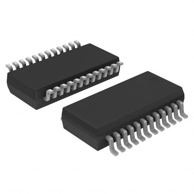
- Package: SOIC (Small Outline Integrated Circuit)
- Essence: Digital multiplexer/demultiplexer with address latches
- Packaging/Quantity: Tape and reel, 2500 units per reel
Specifications
- Supply Voltage Range: 2V to 6V
- Input Voltage Range: GND to VCC
- Operating Temperature Range: -40°C to +125°C
- Output Current: ±25mA
- Propagation Delay Time: 10ns (typical)
Detailed Pin Configuration
- A0: Address input bit 0
- A1: Address input bit 1
- A2: Address input bit 2
- A3: Address input bit 3
- A4: Address input bit 4
- A5: Address input bit 5
- E: Enable input
- Y0: Multiplexer output 0
- Y1: Multiplexer output 1
- Y2: Multiplexer output 2
- Y3: Multiplexer output 3
- Y4: Multiplexer output 4
- Y5: Multiplexer output 5
- Y6: Multiplexer output 6
- Y7: Multiplexer output 7
- VCC: Positive supply voltage
- GND: Ground
Functional Features
- 74HC4059DB,118 is an 8-channel multiplexer/demultiplexer with address latches.
- It can be used to select one of the eight inputs and route it to the output based on the address inputs.
- The address latches allow the selection to be held even when the address inputs change.
- It operates at high speed and consumes low power, making it suitable for various applications.
Advantages
- High-speed operation allows for quick data routing.
- Low power consumption helps in reducing energy usage.
- Address latches ensure stable selection even with changing address inputs.
- Wide supply voltage range (2V to 6V) provides flexibility in different systems.
Disadvantages
- Limited number of input/output channels (8 channels).
- Propagation delay time may affect real-time applications with strict timing requirements.
Working Principles
- The 74HC4059DB,118 uses a combination of address inputs (A0-A5) to select one of the eight multiplexer outputs (Y0-Y7).
- The selected output is determined by the binary value applied to the address inputs.
- The address latches hold the selected output even if the address inputs change.
- The enable input (E) controls the operation of the multiplexer/demultiplexer.
Detailed Application Field Plans
The 74HC4059DB,118 can be used in various applications, including: 1. Data acquisition systems 2. Communication systems 3. Industrial automation 4. Test and measurement equipment 5. Audio/video signal routing
Detailed and Complete Alternative Models
Some alternative models that serve similar functions are: 1. CD4051B: 8-channel analog multiplexer/demultiplexer 2. SN74LS151: 8-line to 1-line data selector/multiplexer 3. MC14051B: 8-channel analog multiplexer/demultiplexer with address latches
Note: These alternative models may have different specifications and pin configurations.
Listen Sie 10 häufige Fragen und Antworten im Zusammenhang mit der Anwendung von 74HC4059DB,118 in technischen Lösungen auf
Sure! Here are 10 common questions and answers related to the application of 74HC4059DB,118 in technical solutions:
Q: What is the 74HC4059DB,118? A: The 74HC4059DB,118 is a high-speed CMOS device that functions as a programmable divide-by-N counter and frequency synthesizer.
Q: What is the maximum operating voltage for the 74HC4059DB,118? A: The maximum operating voltage for the 74HC4059DB,118 is 6 volts.
Q: How many outputs does the 74HC4059DB,118 have? A: The 74HC4059DB,118 has 8 outputs.
Q: Can the 74HC4059DB,118 be used as a frequency divider? A: Yes, the 74HC4059DB,118 can be used as a frequency divider by programming the desired division ratio.
Q: What is the maximum division ratio that can be achieved with the 74HC4059DB,118? A: The maximum division ratio that can be achieved with the 74HC4059DB,118 is 256.
Q: How is the division ratio programmed in the 74HC4059DB,118? A: The division ratio is programmed using external control pins and logic signals.
Q: Can the 74HC4059DB,118 be cascaded to achieve higher division ratios? A: Yes, multiple 74HC4059DB,118 devices can be cascaded to achieve higher division ratios.
Q: What is the typical power consumption of the 74HC4059DB,118? A: The typical power consumption of the 74HC4059DB,118 is low, making it suitable for battery-powered applications.
Q: Can the 74HC4059DB,118 be used in both digital and analog applications? A: The 74HC4059DB,118 is primarily designed for digital applications but can also be used in certain analog applications.
Q: What are some common applications of the 74HC4059DB,118? A: Some common applications of the 74HC4059DB,118 include frequency synthesis, clock generation, frequency division, and signal processing.
Please note that the answers provided here are general and may vary depending on specific datasheet specifications and application requirements.