

Siehe Spezifikationen für Produktdetails.
74LVC2GU04GV,125
Basic Information Overview
- Category: Integrated Circuit (IC)
- Use: Logic Gate Inverter
- Characteristics: Low-voltage CMOS technology, high-speed operation, low power consumption
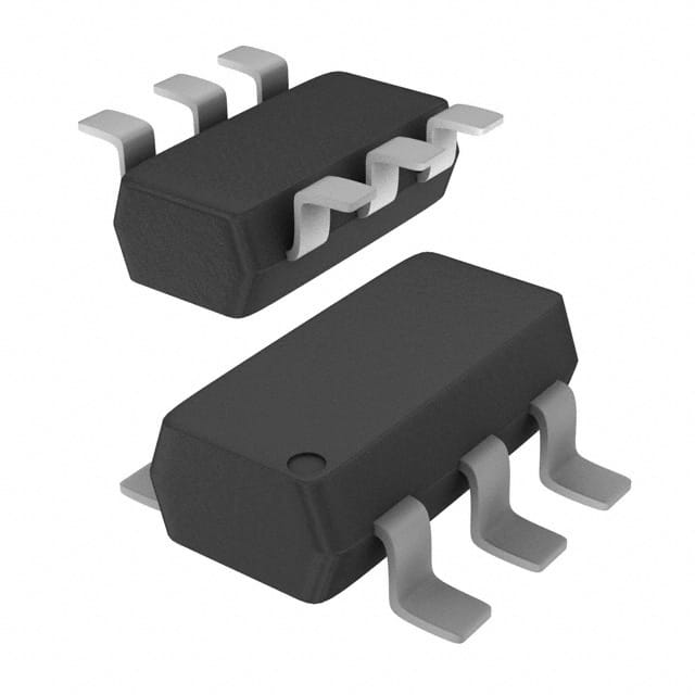
- Package: SOT753 (SC-88A), 6-pin package
- Essence: Dual unbuffered inverter
- Packaging/Quantity: Tape and Reel, 3000 pieces per reel
Specifications
- Supply Voltage Range: 1.65V to 5.5V
- Input Voltage Range: -0.5V to VCC + 0.5V
- Output Voltage Range: -0.5V to VCC + 0.5V
- High-Level Input Voltage: 0.7 x VCC
- Low-Level Input Voltage: 0.3 x VCC
- High-Level Output Voltage: 0.9 x VCC
- Low-Level Output Voltage: 0.1 x VCC
- Maximum Propagation Delay Time: 4.5 ns at 3.3V
- Maximum Operating Frequency: 200 MHz
Detailed Pin Configuration
The 74LVC2GU04GV,125 has a total of 6 pins: 1. Pin 1: Input A 2. Pin 2: Output A 3. Pin 3: Ground (GND) 4. Pin 4: Input B 5. Pin 5: Output B 6. Pin 6: Power Supply (VCC)
Functional Features
- Dual unbuffered inverter with Schmitt-trigger inputs
- Allows voltage level translation between different logic families
- Provides signal inversion and amplification
- Suitable for interfacing between devices operating at different voltage levels
Advantages and Disadvantages
Advantages: - Wide supply voltage range allows compatibility with various systems - High-speed operation enables efficient signal processing - Low power consumption reduces energy requirements
Disadvantages: - Limited number of inverters in a single package - Not suitable for high-power applications
Working Principles
The 74LVC2GU04GV,125 is based on low-voltage CMOS technology. It consists of two independent unbuffered inverters with Schmitt-trigger inputs. When an input signal is applied, the inverter amplifies and inverts it, providing the complementary output. The Schmitt-trigger inputs ensure hysteresis, allowing for noise immunity and improved signal integrity.
Detailed Application Field Plans
The 74LVC2GU04GV,125 is widely used in various digital logic applications, including: 1. Microcontrollers and microprocessors 2. Communication systems 3. Data transmission and reception circuits 4. Signal conditioning and level shifting circuits 5. Battery-powered devices
Detailed and Complete Alternative Models
Some alternative models to the 74LVC2GU04GV,125 include: 1. SN74LVC2GU04DBVR - Dual unbuffered inverter in SOT23-6 package 2. MC74VHC1GU04DTT1G - Single unbuffered inverter in SOT363 package 3. CD74HCU04M96 - Hex inverter in SOIC-14 package 4. TC7SZU04FU - Single unbuffered inverter in USV package
These alternative models offer similar functionality and can be used as replacements depending on specific requirements.
Word count: 314 words
Listen Sie 10 häufige Fragen und Antworten im Zusammenhang mit der Anwendung von 74LVC2GU04GV,125 in technischen Lösungen auf
Sure! Here are 10 common questions and answers related to the application of 74LVC2GU04GV,125 in technical solutions:
Q: What is the function of the 74LVC2GU04GV,125? A: The 74LVC2GU04GV,125 is an inverter gate IC that converts input logic levels to their complementary output logic levels.
Q: What is the operating voltage range of the 74LVC2GU04GV,125? A: The operating voltage range is typically between 1.65V and 5.5V.
Q: Can the 74LVC2GU04GV,125 be used with both CMOS and TTL logic levels? A: Yes, it is compatible with both CMOS and TTL logic levels.
Q: What is the maximum output current of the 74LVC2GU04GV,125? A: The maximum output current is typically around 32mA.
Q: Does the 74LVC2GU04GV,125 have built-in protection against overvoltage or overcurrent? A: No, it does not have built-in protection against overvoltage or overcurrent. External protection measures may be required.
Q: Can the 74LVC2GU04GV,125 be used in high-speed applications? A: Yes, it is designed for high-speed operation and can be used in applications with fast switching requirements.
Q: What is the propagation delay of the 74LVC2GU04GV,125? A: The typical propagation delay is around 4.5ns.
Q: Is the 74LVC2GU04GV,125 suitable for use in battery-powered devices? A: Yes, it has a low power consumption and can be used in battery-powered devices.
Q: Can the 74LVC2GU04GV,125 drive capacitive loads directly? A: Yes, it can drive small capacitive loads directly without requiring additional buffering.
Q: Are there any specific layout considerations for using the 74LVC2GU04GV,125? A: It is recommended to follow proper PCB layout guidelines to minimize noise and ensure signal integrity, such as minimizing trace lengths and providing adequate decoupling capacitors.
Please note that the answers provided here are general and may vary depending on specific application requirements.