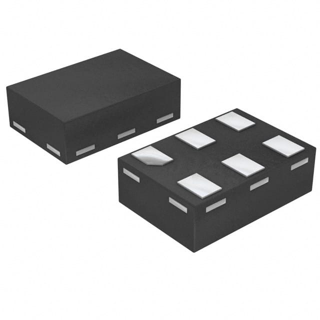
Siehe Spezifikationen für Produktdetails.

74AUP1G0832GM,115
Basic Information Overview
- Category: Integrated Circuit (IC)
- Use: Logic Gate
- Characteristics: Single Schmitt-trigger buffer with open-drain output
- Package: SOT353 (SC-88A)
- Essence: High-speed CMOS technology
- Packaging/Quantity: Tape and Reel, 3000 pieces per reel
Specifications
- Supply Voltage Range: 0.8 V to 3.6 V
- Input Voltage Range: -0.5 V to 4.6 V
- Output Voltage Range: 0 V to VCC + 0.5 V
- Maximum Operating Frequency: 400 MHz
- Propagation Delay: 2.7 ns (typical)
Detailed Pin Configuration
The 74AUP1G0832GM,115 has the following pin configuration:
____
   GND|    |VCC
 IN1_A|    |OUT_A
 IN1_B|    |OUT_B
   GND|____|VCC
Functional Features
- Single Schmitt-trigger buffer with open-drain output
- Wide supply voltage range allows compatibility with various systems
- High-speed operation enables fast signal processing
- Low power consumption for energy-efficient applications
- Open-drain output provides flexibility in interfacing with other devices
Advantages
- Versatile logic gate suitable for a wide range of applications
- Compact package size saves board space
- High-speed operation enhances system performance
- Low power consumption extends battery life in portable devices
- Open-drain output simplifies level shifting and interfacing
Disadvantages
- Limited number of inputs and outputs
- Not suitable for high-voltage applications
- May require additional components for certain circuit configurations
Working Principles
The 74AUP1G0832GM,115 is a single Schmitt-trigger buffer with an open-drain output. It operates based on high-speed CMOS technology, which allows for fast signal processing. The Schmitt-trigger input ensures hysteresis and noise immunity, making it suitable for applications with noisy or slowly changing input signals. The open-drain output provides flexibility in interfacing with other devices by allowing multiple outputs to be connected together.
Detailed Application Field Plans
The 74AUP1G0832GM,115 can be used in various applications, including but not limited to: - Level shifting and voltage translation circuits - Signal conditioning and buffering - Clock distribution networks - Sensor interfaces - Communication systems - Battery-powered devices
Detailed and Complete Alternative Models
Some alternative models that offer similar functionality to the 74AUP1G0832GM,115 include: - SN74LVC1G07DBVR (Texas Instruments) - NC7SZ07P5X (ON Semiconductor) - MC74VHC1GT07DTT1G (ON Semiconductor) - TC7SZ07FU(TE85L,F) (Toshiba)
Please note that the above list is not exhaustive, and there are other alternative models available from different manufacturers.
Word count: 305 words
Listen Sie 10 häufige Fragen und Antworten im Zusammenhang mit der Anwendung von 74AUP1G0832GM,115 in technischen Lösungen auf
Sure! Here are 10 common questions and answers related to the application of 74AUP1G0832GM,115 in technical solutions:
Q1: What is the 74AUP1G0832GM,115? A1: The 74AUP1G0832GM,115 is a single low-power dual-gate analog switch designed for use in various technical applications.
Q2: What is the maximum voltage rating for the 74AUP1G0832GM,115? A2: The maximum voltage rating for the 74AUP1G0832GM,115 is typically around 3.6 volts.
Q3: Can the 74AUP1G0832GM,115 be used as a digital switch? A3: Yes, the 74AUP1G0832GM,115 can be used as a digital switch due to its low-power characteristics and dual-gate design.
Q4: What is the typical power consumption of the 74AUP1G0832GM,115? A4: The typical power consumption of the 74AUP1G0832GM,115 is very low, usually in the microampere range.
Q5: Is the 74AUP1G0832GM,115 suitable for battery-powered applications? A5: Yes, the low-power consumption of the 74AUP1G0832GM,115 makes it well-suited for battery-powered applications where power efficiency is crucial.
Q6: What is the operating temperature range for the 74AUP1G0832GM,115? A6: The operating temperature range for the 74AUP1G0832GM,115 is typically between -40°C to +85°C.
Q7: Can the 74AUP1G0832GM,115 handle both analog and digital signals? A7: Yes, the 74AUP1G0832GM,115 is designed to handle both analog and digital signals effectively.
Q8: What is the typical on-resistance of the 74AUP1G0832GM,115? A8: The typical on-resistance of the 74AUP1G0832GM,115 is very low, usually in the ohm range.
Q9: Can the 74AUP1G0832GM,115 be used in high-frequency applications? A9: Yes, the 74AUP1G0832GM,115 can be used in high-frequency applications due to its fast switching speed and low propagation delay.
Q10: Are there any specific application notes or reference designs available for the 74AUP1G0832GM,115? A10: Yes, the manufacturer provides application notes and reference designs that can help users understand and implement the 74AUP1G0832GM,115 in their technical solutions effectively.
Please note that the answers provided here are general and may vary depending on the specific requirements and conditions of each application.

