

Siehe Spezifikationen für Produktdetails.
A3P030-1QNG48
Product Overview
Category
A3P030-1QNG48 belongs to the category of programmable logic devices (PLDs).
Use
This product is commonly used in digital circuit design and implementation.
Characteristics
- Programmable: The A3P030-1QNG48 can be programmed to perform specific functions.
- Logic Device: It is designed to handle logical operations and data processing.
- High Performance: The device offers fast processing speeds and efficient operation.
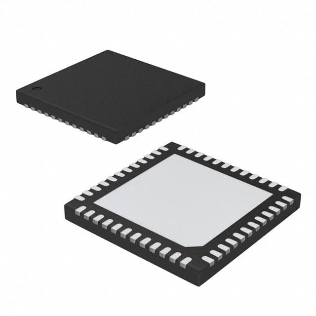
Package
The A3P030-1QNG48 comes in a compact quad flat no-lead (QFN) package.
Essence
The essence of this product lies in its ability to provide flexible and customizable digital circuit solutions.
Packaging/Quantity
The A3P030-1QNG48 is typically packaged individually and is available in various quantities depending on customer requirements.
Specifications
- Model: A3P030-1QNG48
- Package Type: QFN
- Number of Pins: 48
- Operating Voltage: 3.3V
- Maximum Frequency: 100 MHz
- Programmable Logic Cells: 30,000
- I/O Interfaces: 48
Detailed Pin Configuration
The pin configuration for A3P030-1QNG48 is as follows:
| Pin Number | Pin Name | Function | |------------|----------|----------| | 1 | VCC | Power Supply (3.3V) | | 2 | GND | Ground | | 3 | IO0 | Input/Output Pin 0 | | 4 | IO1 | Input/Output Pin 1 | | ... | ... | ... | | 48 | IO47 | Input/Output Pin 47 |
Functional Features
- High-speed operation: The A3P030-1QNG48 offers fast processing capabilities.
- Flexible configuration: It can be programmed to perform a wide range of functions.
- Low power consumption: The device is designed to minimize power usage.
Advantages and Disadvantages
Advantages
- Versatile functionality
- Customizable design
- Compact package size
- Efficient power consumption
Disadvantages
- Limited number of I/O interfaces
- Programming complexity for advanced applications
Working Principles
The A3P030-1QNG48 operates based on the principles of programmable logic. It consists of configurable logic cells that can be interconnected to create desired digital circuits. These logic cells can be programmed using hardware description languages (HDL) or specialized software tools. Once programmed, the device performs the specified logical operations based on the input signals received.
Detailed Application Field Plans
The A3P030-1QNG48 finds applications in various fields, including:
- Industrial Automation: Used for controlling and monitoring processes in manufacturing plants.
- Communication Systems: Employed in network routers and switches for data processing.
- Automotive Electronics: Integrated into vehicle control systems for improved performance.
- Consumer Electronics: Utilized in devices like gaming consoles and smart home appliances.
Detailed and Complete Alternative Models
- A3P060-1TQG144: Similar to A3P030-1QNG48 but with higher logic capacity.
- A3P125-1FG144: Offers increased I/O interfaces and larger programmable logic cells.
- A3P250-2VQG100: Suitable for more complex digital circuit designs with enhanced performance.
These alternative models provide varying specifications and features to cater to different application requirements.
Word count: 399 words
Listen Sie 10 häufige Fragen und Antworten im Zusammenhang mit der Anwendung von A3P030-1QNG48 in technischen Lösungen auf
Sure! Here are 10 common questions and answers related to the application of A3P030-1QNG48 in technical solutions:
1. What is A3P030-1QNG48? A3P030-1QNG48 is a specific model of field-programmable gate array (FPGA) manufactured by Microsemi Corporation.
2. What are the key features of A3P030-1QNG48? Some key features of A3P030-1QNG48 include 30,000 logic elements, 1,152 Kbits of embedded memory, 96 user I/Os, and a maximum operating frequency of 250 MHz.
3. What are the typical applications of A3P030-1QNG48? A3P030-1QNG48 is commonly used in various technical solutions such as industrial automation, telecommunications, automotive electronics, medical devices, and aerospace systems.
4. How can A3P030-1QNG48 be programmed? A3P030-1QNG48 can be programmed using hardware description languages (HDLs) like VHDL or Verilog, which allow users to describe the desired functionality of the FPGA.
5. Can A3P030-1QNG48 be reprogrammed after deployment? Yes, A3P030-1QNG48 is a reprogrammable FPGA, meaning that its configuration can be modified even after it has been deployed in a system.
6. What tools are available for programming A3P030-1QNG48? Microsemi provides Libero SoC Design Suite, which includes software tools for designing, simulating, synthesizing, and programming A3P030-1QNG48.
7. What are the power requirements for A3P030-1QNG48? The power requirements for A3P030-1QNG48 vary depending on the specific application and configuration. It is important to refer to the datasheet and design guidelines provided by Microsemi for accurate power estimation.
8. Can A3P030-1QNG48 interface with other components or devices? Yes, A3P030-1QNG48 supports various communication protocols such as SPI, I2C, UART, and GPIOs, allowing it to interface with other components or devices in a system.
9. Are there any limitations or considerations when using A3P030-1QNG48? Some considerations include the limited number of user I/Os, the available logic resources, and the maximum operating frequency. It is important to carefully analyze the requirements of the specific application to ensure that A3P030-1QNG48 meets the necessary criteria.
10. Where can I find additional technical documentation and support for A3P030-1QNG48? Microsemi provides comprehensive technical documentation, including datasheets, user guides, and application notes, which can be found on their official website. Additionally, they offer customer support through their online forums and direct contact channels.