

Siehe Spezifikationen für Produktdetails.
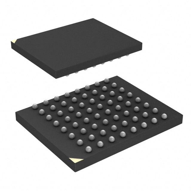
RC28F256P33TFA
Product Overview
- Category: Integrated Circuit
- Use: Memory Storage
- Characteristics: High capacity, fast data access, non-volatile, compact size
- Package: TFA package
- Essence: Flash memory chip
- Packaging/Quantity: Individual units in anti-static packaging
Specifications
- Memory Capacity: 256 Megabits (32 Megabytes)
- Interface: Parallel
- Operating Voltage: 2.7V - 3.6V
- Access Time: 70 ns
- Data Retention: Up to 20 years
- Operating Temperature: -40°C to +85°C
Detailed Pin Configuration
The RC28F256P33TFA has a total of 48 pins. The pin configuration is as follows:
- VCC
- A0
- A1
- A2
- A3
- A4
- A5
- A6
- A7
- A8
- A9
- A10
- A11
- A12
- A13
- A14
- A15
- A16
- A17
- A18
- A19
- A20
- A21
- A22
- A23
- A24
- A25
- A26
- A27
- A28
- A29
- A30
- A31
- CE#
- WE#
- OE#
- BYTE#
- RY/BY#
- WP#
- RESET#
- DQ0
- DQ1
- DQ2
- DQ3
- DQ4
- DQ5
- DQ6
- DQ7
Functional Features
- High-speed data access
- Non-volatile storage
- Low power consumption
- Erase and program operations at the block level
- Built-in hardware write protection
- Reset functionality for system initialization
Advantages and Disadvantages
Advantages: - Large memory capacity - Fast data access - Compact size - Low power consumption - Long data retention period
Disadvantages: - Limited erase and program cycles - Higher cost compared to other memory technologies
Working Principles
The RC28F256P33TFA is based on flash memory technology. It stores data using floating-gate transistors, which can retain their charge even when power is removed. The memory cells are organized into blocks, allowing for efficient erase and program operations. The chip communicates with the host system through a parallel interface, enabling fast data transfer.
Detailed Application Field Plans
The RC28F256P33TFA is widely used in various electronic devices that require non-volatile memory storage. Some of its application fields include:
- Consumer Electronics: Used in digital cameras, MP3 players, and portable gaming devices for storing user data and firmware.
- Automotive Systems: Integrated into car infotainment systems, navigation units, and engine control modules for reliable data storage.
- Industrial Automation: Utilized in programmable logic controllers (PLCs), robotics, and monitoring systems for data logging and configuration storage.
- Networking Equipment: Incorporated into routers, switches, and network appliances for firmware storage and configuration settings.
- Medical Devices: Integrated into medical equipment such as patient monitors and diagnostic devices for storing critical data and software.
Detailed and Complete Alternative Models
- RC28F256P30TFA: Similar to RC28F256P33TFA, but with a lower access time of 30 ns.
- RC28F128P33TFA: Half the memory capacity of RC28F256P33TFA (128 Megabits), suitable for applications with lower storage requirements.
- RC28F512P33TFA: Double the memory capacity of RC28F256P33TFA (512 Megabits), providing more storage space for data-intensive applications.
These alternative models offer different specifications and capacities to cater to diverse application needs.
Word count: 515 words
Listen Sie 10 häufige Fragen und Antworten im Zusammenhang mit der Anwendung von RC28F256P33TFA in technischen Lösungen auf
Sure! Here are 10 common questions and answers related to the application of RC28F256P33TFA in technical solutions:
Q: What is RC28F256P33TFA? A: RC28F256P33TFA is a specific model of flash memory chip manufactured by Intel.
Q: What is the storage capacity of RC28F256P33TFA? A: RC28F256P33TFA has a storage capacity of 256 megabits (32 megabytes).
Q: What is the interface used to connect RC28F256P33TFA to a microcontroller or processor? A: RC28F256P33TFA uses a parallel NOR flash interface.
Q: Can RC28F256P33TFA be used in automotive applications? A: Yes, RC28F256P33TFA is suitable for use in automotive applications due to its high reliability and temperature range.
Q: Is RC28F256P33TFA compatible with 3.3V power supply? A: Yes, RC28F256P33TFA operates on a 3.3V power supply.
Q: What is the maximum operating frequency of RC28F256P33TFA? A: The maximum operating frequency of RC28F256P33TFA is typically 66 MHz.
Q: Does RC28F256P33TFA support hardware data protection features? A: Yes, RC28F256P33TFA supports various hardware data protection features like block locking and password protection.
Q: Can RC28F256P33TFA be used for firmware storage in embedded systems? A: Yes, RC28F256P33TFA is commonly used for firmware storage in embedded systems due to its reliability and high endurance.
Q: What is the typical access time of RC28F256P33TFA? A: The typical access time of RC28F256P33TFA is around 70 ns.
Q: Is RC28F256P33TFA compatible with industry-standard flash memory interfaces? A: Yes, RC28F256P33TFA is compatible with common flash memory interfaces like SPI and parallel NOR flash interfaces.
Please note that the answers provided here are general and may vary depending on specific application requirements and datasheet specifications.