

Siehe Spezifikationen für Produktdetails.
N25Q512A83G1240E
Basic Information Overview
- Category: Non-volatile Memory
- Use: Data storage and retrieval
- Characteristics:
- High capacity
- Fast read/write speeds
- Low power consumption
- Package: Integrated circuit (IC)
- Essence: Flash memory chip
- Packaging/Quantity: Typically sold in trays or reels
Specifications
- Capacity: 512 Megabits (64 Megabytes)
- Interface: Serial Peripheral Interface (SPI)
- Voltage Range: 2.7V to 3.6V
- Operating Temperature Range: -40°C to +85°C
- Erase/Program Operations:
- Sector erase time: 100ms (typical)
- Page program time: 0.7ms (typical)
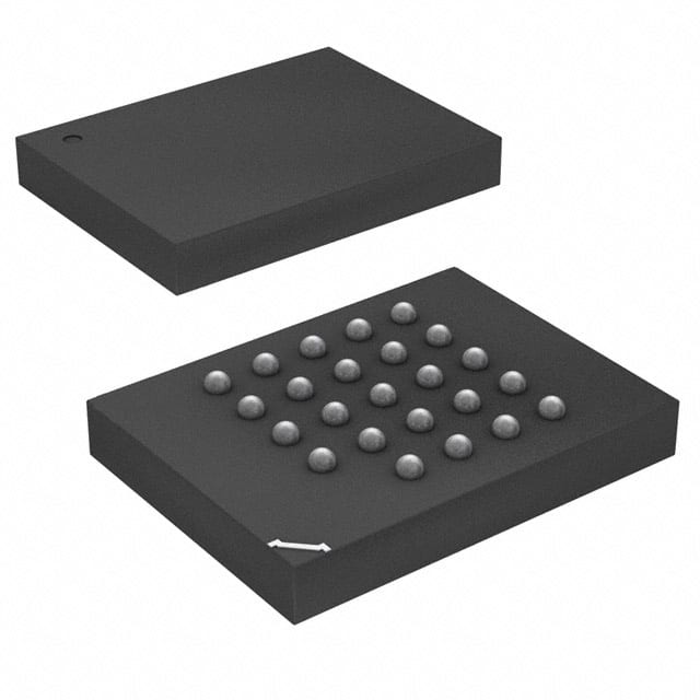
Detailed Pin Configuration
The N25Q512A83G1240E has a total of 8 pins, which are as follows:
- VCC: Power supply voltage input
- GND: Ground reference
- HOLD: Suspends ongoing operations
- WP: Write Protect pin
- IO0: Serial data input/output
- IO1: Serial data input/output
- IO2: Serial data input/output
- IO3: Serial data input/output
Functional Features
- High-speed data transfer using SPI interface
- Efficient sector erase and page program operations
- Flexible write protection options
- Deep power-down mode for low-power applications
- Software and hardware reset functionality
Advantages and Disadvantages
Advantages: - Large storage capacity - Fast read/write speeds - Low power consumption - Compact package size - Versatile write protection options
Disadvantages: - Relatively higher cost compared to other memory technologies - Limited endurance (number of erase/write cycles)
Working Principles
The N25Q512A83G1240E is based on the NAND flash memory technology. It stores data in a series of memory cells organized into pages and sectors. The SPI interface allows for high-speed communication between the chip and the host device. When data needs to be stored or retrieved, the chip performs erase and program operations on specific sectors or pages.
Detailed Application Field Plans
The N25Q512A83G1240E is widely used in various electronic devices that require non-volatile memory for data storage and retrieval. Some common application fields include: - Consumer electronics (e.g., smartphones, tablets, digital cameras) - Automotive systems (e.g., infotainment systems, instrument clusters) - Industrial control systems - Networking equipment - Medical devices
Detailed and Complete Alternative Models
- N25Q256A13EF840E: 256 Megabit capacity, similar features and specifications
- N25Q128A11EF840E: 128 Megabit capacity, similar features and specifications
- N25Q064A13EF840E: 64 Megabit capacity, similar features and specifications
These alternative models offer different capacities while maintaining similar functionality and characteristics to the N25Q512A83G1240E.
Word count: 346 words
Listen Sie 10 häufige Fragen und Antworten im Zusammenhang mit der Anwendung von N25Q512A83G1240E in technischen Lösungen auf
Sure! Here are 10 common questions and answers related to the application of N25Q512A83G1240E in technical solutions:
1. What is N25Q512A83G1240E? - N25Q512A83G1240E is a specific model of flash memory chip manufactured by Micron Technology. It offers a capacity of 512 megabits (64 megabytes) and operates on a 1.8V power supply.
2. What are the main features of N25Q512A83G1240E? - The main features of N25Q512A83G1240E include high-speed read and write operations, low power consumption, advanced security features, and compatibility with various communication interfaces such as SPI and QPI.
3. What are the typical applications of N25Q512A83G1240E? - N25Q512A83G1240E is commonly used in a wide range of applications, including automotive systems, industrial automation, consumer electronics, networking devices, and embedded systems where non-volatile storage is required.
4. What is the maximum operating frequency of N25Q512A83G1240E? - N25Q512A83G1240E supports a maximum operating frequency of up to 133 MHz when using the Serial Peripheral Interface (SPI) mode.
5. Can N25Q512A83G1240E be used for code execution? - Yes, N25Q512A83G1240E can be used for code execution in certain applications. It has a Quad Peripheral Interface (QPI) mode that allows for faster code execution compared to the standard SPI mode.
6. Does N25Q512A83G1240E support hardware and software protection mechanisms? - Yes, N25Q512A83G1240E provides hardware and software protection mechanisms such as write protection, block locking, and password protection to ensure data integrity and prevent unauthorized access.
7. What is the endurance rating of N25Q512A83G1240E? - N25Q512A83G1240E has an endurance rating of 100,000 program/erase cycles per sector, which ensures reliable and long-lasting data storage.
8. Can N25Q512A83G1240E operate in extreme temperature conditions? - Yes, N25Q512A83G1240E is designed to operate in a wide temperature range, typically from -40°C to +85°C, making it suitable for applications that require reliable operation in harsh environments.
9. Is N25Q512A83G1240E compatible with other flash memory devices? - Yes, N25Q512A83G1240E is compatible with other flash memory devices that follow the same industry-standard communication protocols such as SPI and QPI.
10. Are there any specific design considerations when using N25Q512A83G1240E? - When designing with N25Q512A83G1240E, it is important to consider factors such as power supply stability, signal integrity, proper decoupling capacitors, and adherence to the recommended operating conditions mentioned in the datasheet to ensure optimal performance and reliability.