

Siehe Spezifikationen für Produktdetails.
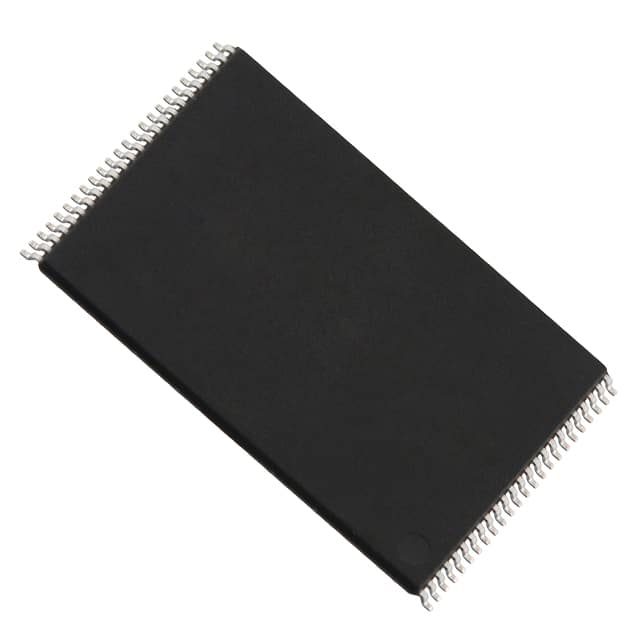
MT29F128G08CFAABWP-12:A
Basic Information Overview
- Category: Memory Device
- Use: Data storage and retrieval
- Characteristics:
- Non-volatile
- High capacity
- Fast read/write speeds
- Package: BGA (Ball Grid Array)
- Essence: Flash memory chip
- Packaging/Quantity: Single chip
Specifications
- Model: MT29F128G08CFAABWP-12:A
- Capacity: 128 GB
- Interface: NAND Flash
- Voltage: 3.3V
- Speed: 12 ns
- Organization: 8 Gb x 16
- Operating Temperature: -40°C to +85°C
Detailed Pin Configuration
The MT29F128G08CFAABWP-12:A has the following pin configuration:
| Pin Number | Pin Name | Description | |------------|----------|-------------| | 1 | VCC | Power supply voltage | | 2 | CE# | Chip enable input | | 3 | CLE | Command latch enable input | | 4 | ALE | Address latch enable input | | 5 | RE# | Read enable input | | 6 | WE# | Write enable input | | 7-22 | A0-A15 | Address inputs | | 23-38 | DQ0-DQ15 | Data inputs/outputs | | 39 | R/B# | Ready/busy output | | 40 | WP# | Write protect input |
Functional Features
- High-speed data transfer
- Reliable and durable
- Error correction capabilities
- Wear-leveling algorithms for extended lifespan
- Block erase and program operations
- Bad block management
Advantages
- Large storage capacity
- Fast read/write speeds
- Low power consumption
- Compact form factor
- High reliability and data integrity
Disadvantages
- Limited endurance (finite number of erase/write cycles)
- Relatively high cost compared to other memory technologies
- Susceptible to data loss in case of power failure during write operations
Working Principles
The MT29F128G08CFAABWP-12:A is based on NAND flash memory technology. It stores data in a series of memory cells organized in a grid-like structure. Each cell can store multiple bits of information, allowing for high-density storage. The data is written and read by applying voltage to specific memory cells. The chip utilizes various algorithms and error correction techniques to ensure data integrity and extend the lifespan of the memory.
Detailed Application Field Plans
The MT29F128G08CFAABWP-12:A is commonly used in various electronic devices that require non-volatile data storage, such as: - Solid-state drives (SSDs) - USB flash drives - Memory cards (SD, microSD, etc.) - Embedded systems - Industrial control systems
Detailed and Complete Alternative Models
- MT29F128G08CBAAAWP-12:A
- MT29F128G08CEAAAWP-12:A
- MT29F128G08CJAAAWP-12:A
- MT29F128G08CKAAAWP-12:A
These alternative models offer similar specifications and functionality, providing options for different application requirements.
Word count: 345 words
Listen Sie 10 häufige Fragen und Antworten im Zusammenhang mit der Anwendung von MT29F128G08CFAABWP-12:A in technischen Lösungen auf
1. What is the MT29F128G08CFAABWP-12:A?
The MT29F128G08CFAABWP-12:A is a specific model of NAND flash memory chip manufactured by Micron Technology.
2. What is the storage capacity of the MT29F128G08CFAABWP-12:A?
The MT29F128G08CFAABWP-12:A has a storage capacity of 128 gigabits (16 gigabytes).
3. What is the operating voltage range for the MT29F128G08CFAABWP-12:A?
The MT29F128G08CFAABWP-12:A operates within a voltage range of 2.7V to 3.6V.
4. What is the maximum data transfer rate supported by the MT29F128G08CFAABWP-12:A?
The MT29F128G08CFAABWP-12:A supports a maximum data transfer rate of 166 megabytes per second.
5. What is the page size of the MT29F128G08CFAABWP-12:A?
The MT29F128G08CFAABWP-12:A has a page size of 8 kilobytes.
6. Does the MT29F128G08CFAABWP-12:A support wear leveling?
Yes, the MT29F128G08CFAABWP-12:A supports wear leveling, which helps distribute write and erase operations evenly across the memory cells to prolong the lifespan of the chip.
7. Is the MT29F128G08CFAABWP-12:A compatible with various interfaces?
Yes, the MT29F128G08CFAABWP-12:A is compatible with common interfaces such as ONFI 2.3, Toggle 2.0, and asynchronous.
8. What is the typical operating temperature range for the MT29F128G08CFAABWP-12:A?
The MT29F128G08CFAABWP-12:A has a typical operating temperature range of -40°C to +85°C.
9. Can the MT29F128G08CFAABWP-12:A be used in automotive applications?
Yes, the MT29F128G08CFAABWP-12:A is designed to meet the requirements of automotive applications and can operate reliably in automotive environments.
10. Does the MT29F128G08CFAABWP-12:A support hardware data protection features?
Yes, the MT29F128G08CFAABWP-12:A supports various hardware data protection features such as ECC (Error Correction Code), bad block management, and internal data scrambling to ensure data integrity and security.