

Siehe Spezifikationen für Produktdetails.
MCP33111D-10T-I/MS
Product Overview
Category
The MCP33111D-10T-I/MS belongs to the category of analog-to-digital converters (ADCs).
Use
This product is primarily used for converting analog signals into digital data, making it suitable for a wide range of applications in various industries.
Characteristics
- High resolution: The MCP33111D-10T-I/MS offers a resolution of 10 bits, ensuring accurate conversion of analog signals.
- Low power consumption: This ADC operates at low power, making it energy-efficient and suitable for battery-powered devices.
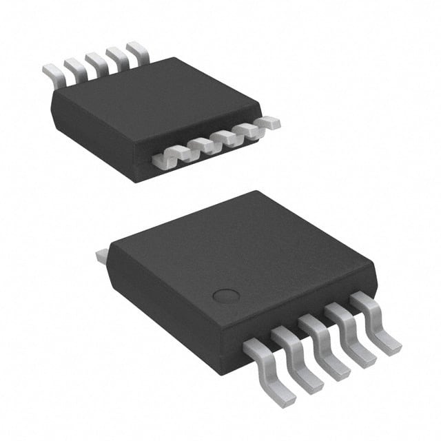
- Small package size: The MCP33111D-10T-I/MS comes in a miniature MSOP-10 package, allowing for space-saving integration into compact designs.
- Wide input voltage range: It can handle input voltages ranging from 0V to VREF, providing flexibility in signal acquisition.
Package and Quantity
The MCP33111D-10T-I/MS is packaged in a MSOP-10 package. Each package contains one unit of the ADC.
Specifications
- Resolution: 10 bits
- Input Voltage Range: 0V to VREF
- Conversion Rate: Up to 500 ksps (thousand samples per second)
- Operating Voltage: 2.7V to 5.5V
- Power Consumption: 150 µA (typical)
- Temperature Range: -40°C to +125°C
Pin Configuration
The MCP33111D-10T-I/MS has the following pin configuration:
- VDD - Power supply voltage
- VREF - Reference voltage for ADC conversion
- VIN+ - Positive analog input voltage
- VIN- - Negative analog input voltage
- CS - Chip select input
- SCLK - Serial clock input
- SDI - Serial data input
- SDO - Serial data output
- DGND - Digital ground
- AGND - Analog ground
Functional Features
- High-speed conversion: The MCP33111D-10T-I/MS can perform conversions at a rate of up to 500 ksps, enabling real-time data acquisition.
- SPI interface: It utilizes a serial peripheral interface (SPI) for communication with microcontrollers or other digital devices.
- Differential inputs: The ADC supports differential input voltage measurements, allowing for accurate and noise-immune signal acquisition.
- Low power standby mode: It features a low-power standby mode, reducing power consumption when not actively converting signals.
Advantages and Disadvantages
Advantages
- High resolution ensures precise analog-to-digital conversion.
- Small package size enables integration into space-constrained designs.
- Wide input voltage range provides flexibility in signal acquisition.
- Low power consumption makes it suitable for battery-powered applications.
- Standby mode reduces power consumption during idle periods.
Disadvantages
- Limited to 10-bit resolution, which may not be sufficient for certain high-precision applications.
- Requires an external reference voltage (VREF) for accurate conversion.
Working Principles
The MCP33111D-10T-I/MS operates based on the successive approximation register (SAR) architecture. It samples the analog input voltage and performs a series of comparisons to determine the digital representation of the input signal. The internal circuitry converts the analog voltage into a binary code, which can then be processed by a microcontroller or other digital devices.
Detailed Application Field Plans
The MCP33111D-10T-I/MS finds applications in various fields, including but not limited to: 1. Industrial automation: Used for monitoring and control systems that require accurate analog-to-digital conversion. 2. Medical devices: Enables precise measurement of physiological signals for diagnostic and monitoring purposes. 3. Automotive electronics: Used in vehicle systems for sensor data acquisition and control. 4. Consumer electronics: Integrated into devices such as audio equipment, digital multimeters, and portable instruments.
Alternative Models
- MCP3201: 12-bit resolution ADC with similar features and package options.
- ADS1115: 16-bit resolution ADC with I2C interface and programmable gain amplification.
- MAX11646: 14-bit resolution ADC with differential inputs and low power consumption.
These alternative models offer different resolutions and interfaces to suit specific application requirements.
In conclusion, the MCP33111D-10T-I/MS is a 10-bit analog-to-digital converter that offers high resolution, low power consumption, and a small package size. It finds applications in various industries and can be used in conjunction with microcontrollers or other digital devices for accurate signal conversion.
Listen Sie 10 häufige Fragen und Antworten im Zusammenhang mit der Anwendung von MCP33111D-10T-I/MS in technischen Lösungen auf
What is the operating voltage range of MCP33111D-10T-I/MS?
- The operating voltage range of MCP33111D-10T-I/MS is 2.7V to 5.5V.What is the resolution of MCP33111D-10T-I/MS?
- MCP33111D-10T-I/MS has a resolution of 10 bits.Can MCP33111D-10T-I/MS be used in industrial control systems?
- Yes, MCP33111D-10T-I/MS is suitable for use in industrial control systems.What is the maximum sampling rate of MCP33111D-10T-I/MS?
- The maximum sampling rate of MCP33111D-10T-I/MS is 500 kilosamples per second (ksps).Is MCP33111D-10T-I/MS compatible with SPI interface?
- Yes, MCP33111D-10T-I/MS supports SPI interface for communication.Can MCP33111D-10T-I/MS be used in battery-powered applications?
- Yes, MCP33111D-10T-I/MS is suitable for battery-powered applications due to its low operating voltage.What is the typical power consumption of MCP33111D-10T-I/MS?
- The typical power consumption of MCP33111D-10T-I/MS is 12.5 mW at 5V.Does MCP33111D-10T-I/MS have built-in programmable gain amplifier (PGA)?
- No, MCP33111D-10T-I/MS does not have a built-in PGA.Is MCP33111D-10T-I/MS suitable for data acquisition systems?
- Yes, MCP33111D-10T-I/MS is well-suited for data acquisition systems.What is the temperature range for MCP33111D-10T-I/MS?
- MCP33111D-10T-I/MS operates within a temperature range of -40°C to +125°C.