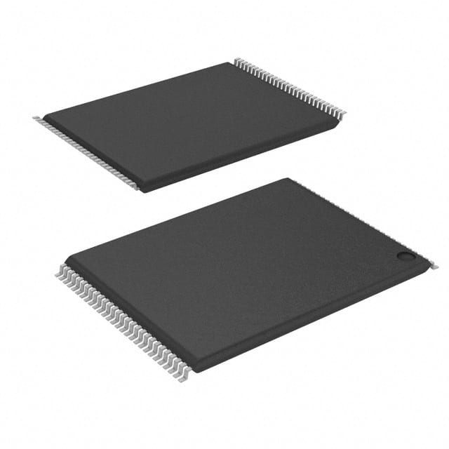
Siehe Spezifikationen für Produktdetails.

MX29GL256FHT2I-90Q
Product Overview
Category
MX29GL256FHT2I-90Q belongs to the category of flash memory chips.
Use
This product is primarily used for data storage in various electronic devices such as smartphones, tablets, digital cameras, and portable media players.
Characteristics
- High storage capacity: MX29GL256FHT2I-90Q offers a storage capacity of 256 megabits (32 megabytes).
- Fast data transfer rate: It supports a high-speed data transfer rate of up to 90 MHz.
- Reliable performance: The flash memory chip ensures reliable and durable data storage.
- Low power consumption: MX29GL256FHT2I-90Q is designed to consume minimal power during operation.
- Compact package: It comes in a small form factor package, making it suitable for space-constrained devices.
- RoHS compliant: This product adheres to the Restriction of Hazardous Substances directive, ensuring environmental safety.
Packaging/Quantity
MX29GL256FHT2I-90Q is typically packaged in trays or reels. Each tray/reel contains a specific quantity of chips, usually ranging from hundreds to thousands, depending on customer requirements.
Specifications
- Manufacturer: MXIC (Macronix International Co., Ltd.)
- Part Number: MX29GL256FHT2I-90Q
- Memory Type: NOR Flash
- Memory Size: 256 Megabits (32 Megabytes)
- Interface: Parallel
- Operating Voltage: 2.7V - 3.6V
- Data Transfer Rate: Up to 90 MHz
- Package Type: TSOP (Thin Small Outline Package)
- Temperature Range: -40°C to +85°C
Detailed Pin Configuration
The MX29GL256FHT2I-90Q flash memory chip has a total of 48 pins. Here is the detailed pin configuration:
- VCC (Power Supply)
- A0-A18 (Address Inputs)
- DQ0-DQ15 (Data Inputs/Outputs)
- WE# (Write Enable)
- CE# (Chip Enable)
- OE# (Output Enable)
- RP#/BYTE# (Reset/Byte Mode Select)
- RY/BY# (Ready/Busy Output)
- WP#/ACC (Write Protect/Acceleration)
- VSS (Ground)
Functional Features
- Erase and Program Operations: MX29GL256FHT2I-90Q supports both sector erase and byte program operations, allowing flexible data manipulation.
- Block Locking: It provides the option to lock specific blocks of memory, preventing accidental modification or erasure.
- Read Operation: The flash memory chip allows fast and reliable reading of stored data.
- High-Speed Interface: With a maximum data transfer rate of 90 MHz, it ensures efficient communication with the host device.
Advantages and Disadvantages
Advantages
- High storage capacity for data-intensive applications.
- Fast data transfer rate enables quick access to stored information.
- Reliable performance ensures data integrity and longevity.
- Low power consumption prolongs battery life in portable devices.
- RoHS compliance promotes environmental sustainability.
Disadvantages
- Limited compatibility with devices that require different memory interfaces.
- Higher cost compared to lower-capacity flash memory chips.
- Susceptible to physical damage if mishandled or exposed to extreme conditions.
Working Principles
MX29GL256FHT2I-90Q utilizes NOR flash memory technology. It stores data by trapping electric charges within floating gate transistors. These charges represent binary values (0 or 1), which can be read, erased, or programmed using specific electrical signals. The memory cells are organized into sectors, allowing efficient data manipulation at the sector level.
Detailed Application Field Plans
MX29GL256FHT2I-90Q finds applications in various electronic devices that require non-volatile storage. Some potential application fields include: - Smartphones and tablets - Digital cameras and camcorders - Portable media players - Automotive infotainment systems - Industrial control systems - Medical devices
Detailed and Complete Alternative Models
- MX29GL128FHT2I-90Q: 128 Megabit (16 Megabyte) flash memory chip with similar specifications.
- MX29GL512FHT2I-90Q: 512 Megabit (64 Megabyte) flash memory chip with higher storage capacity.
- MX29GL1GHT2I-90Q: 1 Gigabit (128 Megabyte) flash memory chip with even higher storage capacity.
These alternative models offer different storage capacities to cater to diverse application requirements.
Word count: 552 words
Listen Sie 10 häufige Fragen und Antworten im Zusammenhang mit der Anwendung von MX29GL256FHT2I-90Q in technischen Lösungen auf
Sure! Here are 10 common questions and answers related to the application of MX29GL256FHT2I-90Q in technical solutions:
Question: What is MX29GL256FHT2I-90Q?
Answer: MX29GL256FHT2I-90Q is a flash memory chip manufactured by Macronix. It has a capacity of 256 megabits (32 megabytes) and operates at a speed of 90 nanoseconds.Question: What are the typical applications of MX29GL256FHT2I-90Q?
Answer: MX29GL256FHT2I-90Q is commonly used in various technical solutions such as embedded systems, consumer electronics, automotive applications, industrial control systems, and more.Question: How does MX29GL256FHT2I-90Q connect to a microcontroller or processor?
Answer: MX29GL256FHT2I-90Q uses a parallel interface to connect to a microcontroller or processor. It typically requires address lines, data lines, control signals, and power supply connections.Question: Can MX29GL256FHT2I-90Q be used for code storage in microcontrollers?
Answer: Yes, MX29GL256FHT2I-90Q can be used for storing program code in microcontrollers. It provides non-volatile storage, allowing the microcontroller to retain the code even when powered off.Question: What is the operating voltage range of MX29GL256FHT2I-90Q?
Answer: MX29GL256FHT2I-90Q operates within a voltage range of 2.7V to 3.6V.Question: Does MX29GL256FHT2I-90Q support random access to data?
Answer: Yes, MX29GL256FHT2I-90Q supports random access to data. It can read or write data at any address within its memory space.Question: Can MX29GL256FHT2I-90Q be reprogrammed multiple times?
Answer: Yes, MX29GL256FHT2I-90Q supports multiple reprogramming cycles. It is designed for frequent read, erase, and write operations.Question: What is the erase time for MX29GL256FHT2I-90Q?
Answer: MX29GL256FHT2I-90Q typically requires a sector erase time of around 1.5 seconds and a chip erase time of around 10 seconds.Question: Does MX29GL256FHT2I-90Q have built-in error correction capabilities?
Answer: No, MX29GL256FHT2I-90Q does not have built-in error correction capabilities. However, it can be used in conjunction with external error correction techniques if required.Question: Is MX29GL256FHT2I-90Q compatible with industry-standard flash memory interfaces?
Answer: Yes, MX29GL256FHT2I-90Q is compatible with common flash memory interfaces such as parallel NOR flash interface, making it easy to integrate into existing systems.
Please note that these answers are general and may vary depending on specific implementation details and requirements.

