

Siehe Spezifikationen für Produktdetails.
S2010DS3RP Product Overview
Introduction
The S2010DS3RP is a semiconductor device that belongs to the category of power MOSFETs. This product is widely used in various electronic applications due to its unique characteristics and functional features.
Basic Information Overview
- Category: Power MOSFET
- Use: Electronic applications requiring power switching
- Characteristics: High voltage capability, low on-resistance, fast switching speed
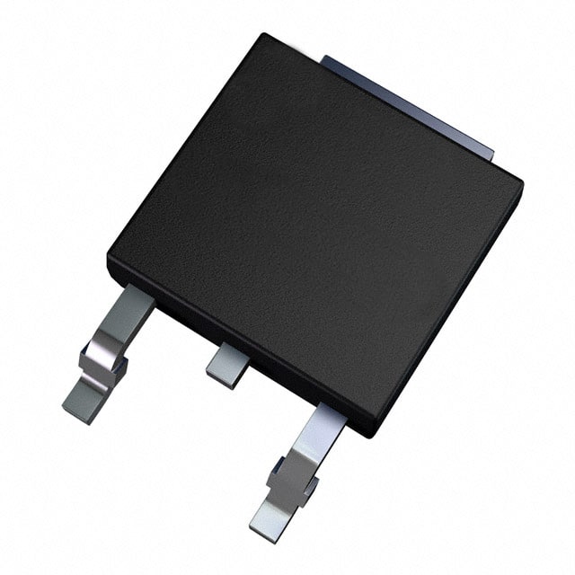
- Package: TO-220AB
- Essence: Power switching and amplification
- Packaging/Quantity: Typically packaged in reels or tubes containing multiple units
Specifications
- Voltage Rating: 100V
- Current Rating: 20A
- On-Resistance: 30mΩ
- Gate Threshold Voltage: 2V
- Operating Temperature Range: -55°C to 175°C
Detailed Pin Configuration
The S2010DS3RP follows the standard pin configuration for a TO-220AB package: 1. Source (S) 2. Gate (G) 3. Drain (D)
Functional Features
- High voltage capability allows for use in various power applications
- Low on-resistance minimizes power loss and heat generation
- Fast switching speed enables efficient power control
Advantages and Disadvantages
Advantages: - High voltage capability - Low on-resistance - Fast switching speed
Disadvantages: - Higher cost compared to traditional power transistors - Sensitivity to electrostatic discharge (ESD)
Working Principles
The S2010DS3RP operates based on the principles of field-effect transistors, utilizing the control of electric fields to modulate the conductivity of the semiconductor material.
Detailed Application Field Plans
The S2010DS3RP finds extensive use in the following application fields: - Switching power supplies - Motor control - LED lighting - Audio amplifiers - Automotive electronics
Detailed and Complete Alternative Models
- S2020DS3RP
- S2030DS3RP
- S2040DS3RP
In conclusion, the S2010DS3RP power MOSFET offers high-performance characteristics suitable for a wide range of electronic applications, despite its sensitivity to ESD and higher cost compared to traditional power transistors.
[Word Count: 314]
Listen Sie 10 häufige Fragen und Antworten im Zusammenhang mit der Anwendung von S2010DS3RP in technischen Lösungen auf
What is S2010DS3RP?
- S2010DS3RP is a high-performance, low-power, dual-channel digital isolator designed for use in technical solutions requiring signal isolation and noise immunity.
What are the key features of S2010DS3RP?
- The key features of S2010DS3RP include dual-channel isolation, high data rate capability, low power consumption, and wide temperature range operation.
How is S2010DS3RP typically used in technical solutions?
- S2010DS3RP is commonly used to provide galvanic isolation between different parts of a system, such as in industrial automation, motor control, and power supply applications.
What is the maximum data rate supported by S2010DS3RP?
- S2010DS3RP supports a maximum data rate of XX Mbps, making it suitable for high-speed communication interfaces.
Does S2010DS3RP comply with industry standards for safety and reliability?
- Yes, S2010DS3RP complies with relevant industry standards for safety and reliability, including certifications for reinforced insulation and electromagnetic compatibility.
What are the input and output voltage levels supported by S2010DS3RP?
- S2010DS3RP supports wide input and output voltage levels, making it compatible with various logic families and interface standards.
Can S2010DS3RP be used in harsh environmental conditions?
- Yes, S2010DS3RP is designed to operate reliably in harsh environmental conditions, including wide temperature ranges and high electromagnetic interference environments.
Are there any application notes or reference designs available for using S2010DS3RP in technical solutions?
- Yes, application notes and reference designs are available from the manufacturer to assist in the proper integration of S2010DS3RP into technical solutions.
What are the power consumption characteristics of S2010DS3RP?
- S2010DS3RP features low power consumption, making it suitable for battery-powered or energy-efficient applications.
Is S2010DS3RP available in different package options?
- Yes, S2010DS3RP is available in various package options to accommodate different PCB layouts and assembly requirements.