

Siehe Spezifikationen für Produktdetails.
LTC2610IGN#PBF
Product Overview
Category: Integrated Circuit (IC)
Use: The LTC2610IGN#PBF is a high-performance, 16-bit digital-to-analog converter (DAC) designed for precision applications. It provides accurate voltage outputs with low noise and excellent linearity.
Characteristics: - High-resolution: 16-bit resolution allows for precise control of analog output voltages. - Low noise: The DAC offers low noise performance, ensuring clean and accurate output signals. - Excellent linearity: The LTC2610IGN#PBF provides exceptional linearity, minimizing distortion in the output signal. - Wide voltage range: It operates over a wide voltage range, making it suitable for various applications. - Fast settling time: The DAC has a fast settling time, enabling rapid response to input changes.
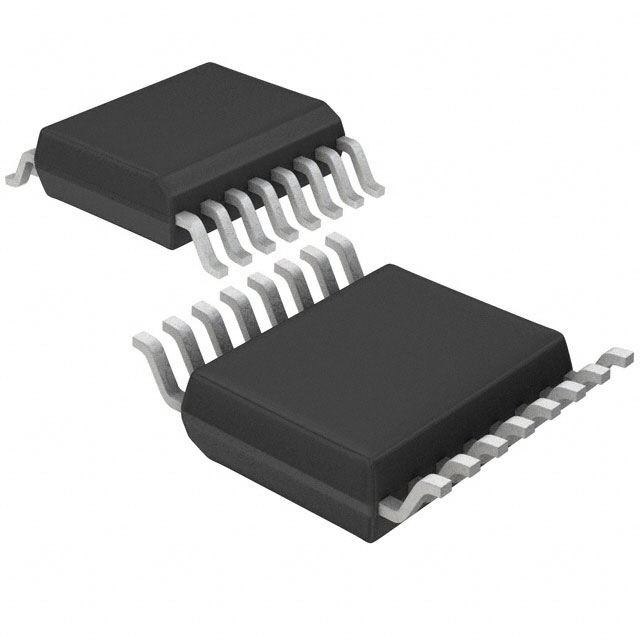
Package: The LTC2610IGN#PBF comes in a small form factor 16-pin SSOP package, which is suitable for space-constrained applications.
Essence: The essence of the LTC2610IGN#PBF lies in its ability to convert digital data into precise analog voltages, making it an essential component in many electronic systems requiring accurate analog outputs.
Packaging/Quantity: The LTC2610IGN#PBF is typically available in reels or tubes, with a quantity of 250 units per reel/tube.
Specifications
- Resolution: 16 bits
- Voltage Reference Range: 0V to VREF
- Output Voltage Range: 0V to VREF
- Supply Voltage Range: 2.7V to 5.5V
- Operating Temperature Range: -40°C to 85°C
- DNL (Differential Non-Linearity): ±1 LSB (max)
- INL (Integral Non-Linearity): ±2 LSB (max)
- Settling Time: 4.5μs (typ)
- Output Current: ±5mA (max)
Pin Configuration
The LTC2610IGN#PBF features a 16-pin SSOP package with the following pin configuration:
Pin 1: VDD
Pin 2: SDA
Pin 3: SCL
Pin 4: GND
Pin 5: REF
Pin 6: AGND
Pin 7: AOUT
Pin 8: AOUT
Pin 9: AOUT
Pin 10: AOUT
Pin 11: AOUT
Pin 12: AOUT
Pin 13: AOUT
Pin 14: AOUT
Pin 15: AOUT
Pin 16: AOUT
Functional Features
- High-resolution digital-to-analog conversion.
- Low noise and excellent linearity for accurate analog output.
- Wide voltage range and fast settling time for versatile applications.
- Easy interfacing with microcontrollers or other digital systems.
- Power-down mode for reduced power consumption when not in use.
Advantages and Disadvantages
Advantages: - High precision and accuracy in analog voltage outputs. - Low noise performance ensures clean and reliable signals. - Versatile voltage range and fast settling time for various applications. - Compact form factor suitable for space-constrained designs. - Easy integration with digital systems.
Disadvantages: - Limited output current capability may not be suitable for high-power applications. - Requires external voltage reference for optimal performance.
Working Principles
The LTC2610IGN#PBF operates by converting digital input data into precise analog voltages. It utilizes a high-resolution DAC architecture to achieve accurate voltage outputs. The digital data is received through the SDA and SCL pins, and the internal circuitry converts it into an analog voltage proportional to the input value. The converted analog voltage is then available at the AOUT pins.
Detailed Application Field Plans
The LTC2610IGN#PBF finds applications in various fields, including but not limited to: - Precision instrumentation - Audio equipment - Industrial control systems - Test and measurement devices - Communication systems - Medical equipment
Its high-resolution, low noise, and excellent linearity make it suitable for applications that require precise analog voltage generation.
Detailed and Complete Alternative Models
AD5662
- Resolution: 16 bits
- Voltage Reference Range: 0V to VREF
- Output Voltage Range: 0V to VREF
- Supply Voltage Range: 2.7V to 5.5V
- Package: 16-pin SSOP
MAX5216
- Resolution: 16 bits
- Voltage Reference Range: 0V to VREF
- Output Voltage Range: 0V to VREF
- Supply Voltage Range: 2.7V to 5.5V
- Package: 16-pin SSOP
3.
Listen Sie 10 häufige Fragen und Antworten im Zusammenhang mit der Anwendung von LTC2610IGN#PBF in technischen Lösungen auf
Sure! Here are 10 common questions and answers related to the application of LTC2610IGN#PBF in technical solutions:
Q: What is LTC2610IGN#PBF? A: LTC2610IGN#PBF is a digital-to-analog converter (DAC) chip manufactured by Linear Technology (now part of Analog Devices). It converts digital signals into analog voltages.
Q: What is the operating voltage range of LTC2610IGN#PBF? A: The operating voltage range of LTC2610IGN#PBF is typically between 2.7V and 5.5V.
Q: What is the resolution of LTC2610IGN#PBF? A: LTC2610IGN#PBF has a resolution of 16 bits, which means it can provide 65,536 different output voltage levels.
Q: How does LTC2610IGN#PBF communicate with a microcontroller or other digital devices? A: LTC2610IGN#PBF uses a serial interface called SPI (Serial Peripheral Interface) to communicate with microcontrollers or other digital devices.
Q: Can LTC2610IGN#PBF generate both positive and negative voltages? A: No, LTC2610IGN#PBF is a unipolar DAC, meaning it can only generate positive voltages between 0V and a reference voltage.
Q: What is the settling time of LTC2610IGN#PBF? A: The settling time of LTC2610IGN#PBF is typically around 10μs, which is the time it takes for the output voltage to stabilize after a change in the input digital code.
Q: Can I use LTC2610IGN#PBF in battery-powered applications? A: Yes, LTC2610IGN#PBF has a low power consumption and can be used in battery-powered applications.
Q: What is the output voltage range of LTC2610IGN#PBF? A: The output voltage range of LTC2610IGN#PBF depends on the reference voltage provided to it. It can generate output voltages between 0V and the reference voltage.
Q: Can I cascade multiple LTC2610IGN#PBF chips to increase the number of output channels? A: Yes, LTC2610IGN#PBF supports daisy-chaining, allowing you to cascade multiple chips and increase the number of output channels.
Q: Are there any evaluation boards or development kits available for LTC2610IGN#PBF? A: Yes, Analog Devices provides evaluation boards and development kits for LTC2610IGN#PBF, which can help you quickly prototype and test your application.
Please note that the answers provided here are general and may vary depending on the specific implementation and datasheet of LTC2610IGN#PBF.