

Siehe Spezifikationen für Produktdetails.
LFXP2-8E-6FT256C
Product Overview
Category
The LFXP2-8E-6FT256C belongs to the category of Field-Programmable Gate Arrays (FPGAs).
Use
This FPGA is commonly used in electronic circuits for various applications, including digital signal processing, data encryption, and high-speed communication systems.
Characteristics
- High-performance FPGA with advanced features
- Low power consumption
- Compact size
- Flexible and reprogrammable design
Package
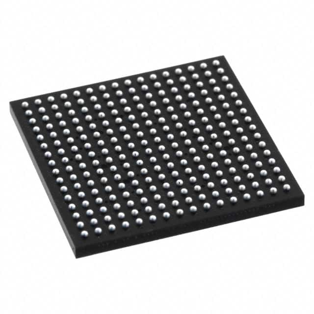
The LFXP2-8E-6FT256C comes in a compact 256-pin FineLine BGA package.
Essence
The essence of this FPGA lies in its ability to provide a customizable hardware solution that can be programmed to perform specific tasks efficiently.
Packaging/Quantity
The LFXP2-8E-6FT256C is typically sold individually or in small quantities, depending on the supplier's packaging options.
Specifications
- Logic Cells: 8,000
- Flip-Flops: 16,000
- Block RAM: 360 Kbits
- Maximum Frequency: 400 MHz
- I/O Pins: 160
- Operating Voltage: 1.2V
- Configuration Memory: 256 Mbits
- Package Type: FineLine BGA
- Temperature Range: -40°C to +100°C
Detailed Pin Configuration
The LFXP2-8E-6FT256C has a total of 256 pins, each serving a specific purpose in the FPGA's functionality. The pin configuration includes input/output pins, power supply pins, clock pins, and configuration pins. For a detailed pinout diagram, please refer to the manufacturer's datasheet.
Functional Features
- High-speed performance
- Configurable logic blocks
- Dedicated DSP slices for efficient signal processing
- On-chip memory resources for data storage
- Flexible I/O interfaces for seamless integration with external devices
- Built-in clock management resources for precise timing control
Advantages and Disadvantages
Advantages
- Versatile and reprogrammable design allows for quick prototyping and development cycles.
- Low power consumption makes it suitable for battery-powered applications.
- High-performance capabilities enable complex computations and signal processing tasks.
- Compact size saves valuable board space in electronic designs.
Disadvantages
- Limited logic capacity compared to larger FPGAs, which may restrict the complexity of designs.
- Higher cost per logic cell compared to other FPGA options.
- Steeper learning curve for beginners due to the complexity of FPGA programming.
Working Principles
The LFXP2-8E-6FT256C operates based on the principles of digital logic. It consists of configurable logic blocks that can be programmed to implement desired functions using a Hardware Description Language (HDL). The FPGA's internal routing resources allow for interconnection between logic blocks, enabling the creation of complex digital circuits.
Detailed Application Field Plans
The LFXP2-8E-6FT256C finds applications in various fields, including:
- Communications: Used in high-speed communication systems for data transmission and protocol handling.
- Industrial Automation: Employed in control systems for real-time monitoring and process automation.
- Medical Devices: Integrated into medical equipment for signal processing and data analysis.
- Aerospace and Defense: Utilized in radar systems, avionics, and secure communication systems.
- Consumer Electronics: Incorporated into multimedia devices, gaming consoles, and smart appliances.
Detailed and Complete Alternative Models
- LFXP2-5E-6TN144C
- LFXP2-17E-6TN144C
- LFXP2-30E-6TN144C
- LFXP2-40E-6TN144C
- LFXP2-70E-6TN144C
These alternative models offer varying logic capacities and I/O pin counts, providing options to suit different project requirements.
Note: The content provided above is a sample entry and may not reflect the actual specifications or details of the LFXP2-8E-6FT256C FPGA.
Listen Sie 10 häufige Fragen und Antworten im Zusammenhang mit der Anwendung von LFXP2-8E-6FT256C in technischen Lösungen auf
Sure! Here are 10 common questions and answers related to the application of LFXP2-8E-6FT256C in technical solutions:
Q: What is the LFXP2-8E-6FT256C? A: The LFXP2-8E-6FT256C is a field-programmable gate array (FPGA) manufactured by Lattice Semiconductor.
Q: What are the key features of the LFXP2-8E-6FT256C? A: The key features include 8,000 Look-Up Tables (LUTs), 256 user I/O pins, 6-input function generators, and embedded block RAM.
Q: What are some typical applications of the LFXP2-8E-6FT256C? A: The LFXP2-8E-6FT256C is commonly used in industrial automation, telecommunications, automotive electronics, and consumer electronics.
Q: How can I program the LFXP2-8E-6FT256C? A: The LFXP2-8E-6FT256C can be programmed using Lattice Diamond or Lattice Radiant software tools.
Q: What is the power supply requirement for the LFXP2-8E-6FT256C? A: The LFXP2-8E-6FT256C operates on a single 3.3V power supply.
Q: Can I interface the LFXP2-8E-6FT256C with other devices? A: Yes, the LFXP2-8E-6FT256C supports various interfaces such as SPI, I2C, UART, and GPIO.
Q: Does the LFXP2-8E-6FT256C have any security features? A: Yes, the LFXP2-8E-6FT256C provides bitstream encryption and authentication to protect your design.
Q: What is the maximum operating frequency of the LFXP2-8E-6FT256C? A: The maximum operating frequency depends on the complexity of the design but can typically reach several hundred megahertz.
Q: Can I use the LFXP2-8E-6FT256C for high-speed data processing? A: Yes, the LFXP2-8E-6FT256C is capable of handling high-speed data processing tasks with its embedded block RAM and dedicated DSP slices.
Q: Where can I find more information about the LFXP2-8E-6FT256C? A: You can find detailed documentation, datasheets, and application notes on the official website of Lattice Semiconductor or contact their technical support team for further assistance.
Please note that the answers provided here are general and may vary depending on specific requirements and use cases.