

Siehe Spezifikationen für Produktdetails.
LFXP2-8E-5MN132I
Product Overview
Category
LFXP2-8E-5MN132I belongs to the category of Field Programmable Gate Arrays (FPGAs).
Use
This product is primarily used in digital logic circuits for various applications such as telecommunications, automotive electronics, industrial automation, and consumer electronics.
Characteristics
- High-performance FPGA with advanced features
- Low power consumption
- Flexible and reconfigurable design
- High-speed data processing capabilities
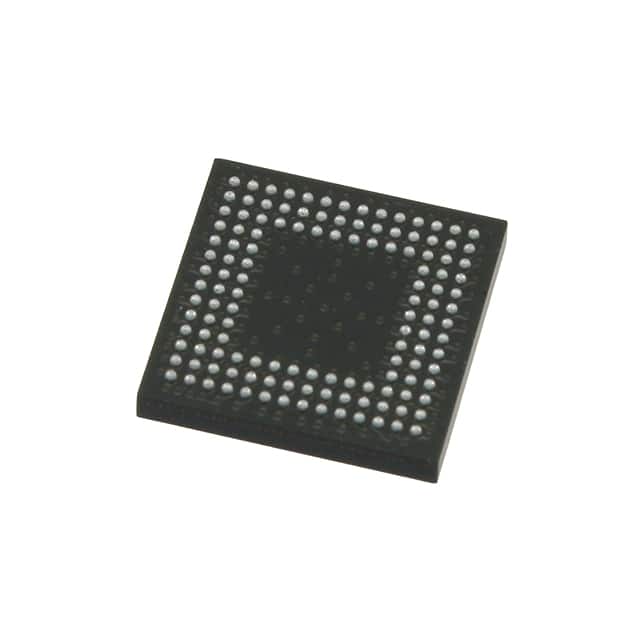
Package
LFXP2-8E-5MN132I comes in a compact package that ensures easy integration into electronic systems. The package provides protection against environmental factors and facilitates efficient heat dissipation.
Essence
The essence of LFXP2-8E-5MN132I lies in its ability to provide a customizable and versatile solution for complex digital circuit designs. It offers a high level of performance and flexibility, making it suitable for a wide range of applications.
Packaging/Quantity
LFXP2-8E-5MN132I is typically packaged in trays or reels, depending on the quantity ordered. The packaging ensures safe transportation and storage of the product.
Specifications
- Logic Cells: 8,000
- Maximum Frequency: 400 MHz
- Embedded Memory: 1,320 Kbits
- I/O Pins: 132
- Operating Voltage: 1.2V
- Package Type: QFN
Detailed Pin Configuration
The pin configuration of LFXP2-8E-5MN132I is as follows:
| Pin Number | Pin Name | Description | |------------|----------|-------------| | 1 | VCCINT | Power supply voltage for internal circuitry | | 2 | GND | Ground | | 3 | IOB0 | Input/output pin | | 4 | IOB1 | Input/output pin | | ... | ... | ... | | 132 | IOB_131 | Input/output pin |
Functional Features
- Configurable logic blocks for implementing complex digital functions
- Dedicated high-speed I/Os for efficient data transfer
- On-chip memory for storing configuration data
- Clock management resources for precise timing control
- Built-in DSP blocks for signal processing tasks
- Support for various communication protocols
Advantages and Disadvantages
Advantages
- High-performance FPGA with advanced features
- Flexible and reconfigurable design allows for easy modifications
- Low power consumption, making it suitable for battery-powered devices
- Wide range of applications due to its versatility
- Excellent data processing capabilities
Disadvantages
- Relatively higher cost compared to other programmable logic devices
- Steeper learning curve for beginners due to its complexity
- Limited availability of alternative models from different manufacturers
Working Principles
LFXP2-8E-5MN132I operates based on the principles of field-programmable gate arrays. It consists of configurable logic blocks (CLBs), interconnect resources, and input/output blocks (IOBs). The CLBs can be programmed to implement desired digital functions using a hardware description language (HDL) or a graphical user interface (GUI). The interconnect resources provide routing paths between different CLBs and IOBs, enabling data flow within the FPGA. The IOBs facilitate communication between the FPGA and external devices.
Detailed Application Field Plans
LFXP2-8E-5MN132I finds applications in various fields, including:
- Telecommunications: Used in network equipment, base stations, and routers for high-speed data processing and protocol handling.
- Automotive Electronics: Employed in automotive control systems, infotainment systems, and driver assistance systems for efficient data processing and control.
- Industrial Automation: Utilized in programmable logic controllers (PLCs), motor control systems, and robotics for precise control and automation tasks.
- Consumer Electronics: Integrated into smart TVs, gaming consoles, and home automation systems to enable advanced functionalities and connectivity.
Detailed and Complete Alternative Models
While LFXP2-8E-5MN132I is a highly capable FPGA, there are alternative models available from different manufacturers that offer similar functionality. Some notable alternatives include:
- Xilinx Artix-7
- Intel Cyclone V
- Microchip PolarFire
- Lattice ECP5
These alternative models provide a range of options with varying performance levels, power consumption, and pricing, allowing designers to choose the most suitable FPGA for their specific requirements.
Word count: 615 words
Listen Sie 10 häufige Fragen und Antworten im Zusammenhang mit der Anwendung von LFXP2-8E-5MN132I in technischen Lösungen auf
Sure! Here are 10 common questions and answers related to the application of LFXP2-8E-5MN132I in technical solutions:
Q: What is the LFXP2-8E-5MN132I? A: The LFXP2-8E-5MN132I is a field-programmable gate array (FPGA) manufactured by Lattice Semiconductor.
Q: What are the key features of the LFXP2-8E-5MN132I? A: The key features include 8,000 Look-Up Tables (LUTs), 132 I/O pins, low power consumption, and high-speed performance.
Q: In what applications can the LFXP2-8E-5MN132I be used? A: The LFXP2-8E-5MN132I can be used in various applications such as industrial automation, automotive electronics, telecommunications, and consumer electronics.
Q: How does the LFXP2-8E-5MN132I help in industrial automation? A: The FPGA can be programmed to control and monitor processes, interface with sensors and actuators, and implement complex algorithms for automation systems.
Q: Can the LFXP2-8E-5MN132I be used in automotive electronics? A: Yes, the FPGA can be utilized in automotive applications for functions like advanced driver assistance systems (ADAS), infotainment systems, and engine control units (ECUs).
Q: What advantages does the LFXP2-8E-5MN132I offer in telecommunications? A: The FPGA provides flexibility to implement custom protocols, signal processing algorithms, and network interfaces required in telecommunications equipment.
Q: How does the LFXP2-8E-5MN132I benefit consumer electronics? A: The FPGA can be used to develop high-performance audio/video processing, gaming consoles, smart home devices, and other consumer electronic products.
Q: Can the LFXP2-8E-5MN132I interface with external devices? A: Yes, the FPGA has 132 I/O pins that can be used to connect and communicate with various external devices such as sensors, displays, memory, and communication interfaces.
Q: What programming languages are supported by the LFXP2-8E-5MN132I? A: The FPGA can be programmed using hardware description languages (HDLs) like VHDL or Verilog, as well as higher-level design tools provided by Lattice Semiconductor.
Q: Are there any development kits available for the LFXP2-8E-5MN132I? A: Yes, Lattice Semiconductor offers development kits and software tools specifically designed for the LFXP2-8E-5MN132I FPGA, making it easier to prototype and develop applications.
Please note that the answers provided here are general and may vary depending on specific requirements and use cases.