

Siehe Spezifikationen für Produktdetails.
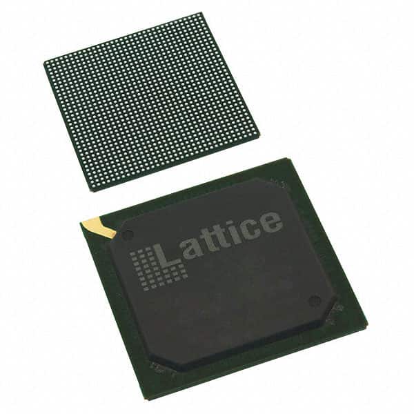
LFE3-70EA-8LFN1156I
Product Overview
Category
The LFE3-70EA-8LFN1156I belongs to the category of Field Programmable Gate Arrays (FPGAs).
Use
This FPGA is commonly used in electronic circuits for digital logic design, prototyping, and implementation of complex digital systems.
Characteristics
- High-performance programmable logic device
- Offers flexibility and reconfigurability
- Provides high-speed data processing capabilities
- Supports a wide range of applications
Package
The LFE3-70EA-8LFN1156I comes in a compact package that ensures easy integration into electronic circuit boards.
Essence
The essence of this FPGA lies in its ability to provide a customizable hardware platform for implementing various digital designs.
Packaging/Quantity
The LFE3-70EA-8LFN1156I is typically packaged individually and is available in varying quantities depending on the manufacturer's specifications.
Specifications
- Model: LFE3-70EA-8LFN1156I
- Logic Elements: 70,000
- Flip-Flops: 1,080,000
- Embedded Memory: 4.9 Mb
- DSP Blocks: 360
- Maximum User I/Os: 1,156
- Operating Voltage: 1.2V
- Speed Grade: -8
- Package Type: BGA
Detailed Pin Configuration
The LFE3-70EA-8LFN1156I has a comprehensive pin configuration, including input/output pins, power supply pins, and configuration pins. For a detailed pinout diagram, please refer to the manufacturer's datasheet.
Functional Features
- High-speed data processing capabilities
- Configurable logic elements for custom designs
- Embedded memory blocks for efficient data storage
- Digital Signal Processing (DSP) blocks for signal processing tasks
- Flexible I/O options for interfacing with external devices
Advantages and Disadvantages
Advantages
- Flexibility and reconfigurability allow for rapid prototyping and design iterations
- High-performance capabilities enable complex digital system implementation
- Wide range of applications, including telecommunications, automotive, aerospace, and more
Disadvantages
- Steep learning curve for beginners due to the complexity of FPGA programming
- Higher cost compared to other programmable logic devices
- Limited availability of alternative models with similar specifications
Working Principles
The LFE3-70EA-8LFN1156I operates based on the principles of configurable logic elements, which can be programmed to perform specific functions. These logic elements are interconnected through a network of programmable interconnects, allowing for the creation of complex digital circuits.
Detailed Application Field Plans
The LFE3-70EA-8LFN1156I finds applications in various fields, including:
- Telecommunications: Used in base stations, routers, and network switches for high-speed data processing.
- Automotive: Employed in advanced driver-assistance systems (ADAS) and infotainment systems for enhanced functionality.
- Aerospace: Utilized in avionics systems for reliable and efficient data processing in aircraft.
Detailed and Complete Alternative Models
While the LFE3-70EA-8LFN1156I is a highly capable FPGA, there are alternative models available with similar specifications. Some notable alternatives include:
- Xilinx Virtex UltraScale+ VU9P FPGA
- Intel Stratix 10 GX FPGA
- Microsemi PolarFire FPGA
These alternative models offer comparable performance and features, providing users with a range of options for their specific application requirements.
Word count: 443 words
Listen Sie 10 häufige Fragen und Antworten im Zusammenhang mit der Anwendung von LFE3-70EA-8LFN1156I in technischen Lösungen auf
Sure! Here are 10 common questions and answers related to the application of LFE3-70EA-8LFN1156I in technical solutions:
Q: What is the LFE3-70EA-8LFN1156I? A: The LFE3-70EA-8LFN1156I is a field-programmable gate array (FPGA) manufactured by Lattice Semiconductor.
Q: What are the key features of the LFE3-70EA-8LFN1156I? A: The key features include 70,000 lookup tables (LUTs), 1,156 user I/O pins, high-speed SERDES channels, embedded memory blocks, and low power consumption.
Q: What applications can the LFE3-70EA-8LFN1156I be used for? A: The LFE3-70EA-8LFN1156I can be used in various applications such as telecommunications, networking, industrial automation, automotive, and aerospace.
Q: How can I program the LFE3-70EA-8LFN1156I? A: The LFE3-70EA-8LFN1156I can be programmed using Lattice Diamond design software or other compatible programming tools.
Q: What is the maximum operating frequency of the LFE3-70EA-8LFN1156I? A: The maximum operating frequency of the LFE3-70EA-8LFN1156I depends on the specific design and implementation, but it can typically reach several hundred megahertz (MHz) or even gigahertz (GHz).
Q: Can the LFE3-70EA-8LFN1156I interface with external devices? A: Yes, the LFE3-70EA-8LFN1156I has a large number of user I/O pins that can be used to interface with external devices such as sensors, displays, memory, and communication interfaces.
Q: Does the LFE3-70EA-8LFN1156I support high-speed serial communication? A: Yes, the LFE3-70EA-8LFN1156I includes high-speed SERDES channels that support protocols like PCIe, SATA, USB, Ethernet, and more.
Q: What is the power consumption of the LFE3-70EA-8LFN1156I? A: The power consumption of the LFE3-70EA-8LFN1156I depends on the specific design and usage, but it is designed to be low power and energy-efficient.
Q: Can the LFE3-70EA-8LFN1156I be reprogrammed multiple times? A: Yes, the LFE3-70EA-8LFN1156I is a field-programmable device, which means it can be reprogrammed multiple times to implement different designs or updates.
Q: Are there any development boards or evaluation kits available for the LFE3-70EA-8LFN1156I? A: Yes, Lattice Semiconductor provides development boards and evaluation kits specifically designed for the LFE3-70EA-8LFN1156I, which can help in prototyping and testing applications.