

Siehe Spezifikationen für Produktdetails.
LFE2M70SE-6F900C
Product Overview
Category
The LFE2M70SE-6F900C belongs to the category of Field Programmable Gate Arrays (FPGAs).
Use
This product is primarily used in digital logic circuits for various applications such as telecommunications, automotive, industrial automation, and consumer electronics.
Characteristics
- High-performance FPGA with advanced features
- Low power consumption
- Large capacity for complex designs
- Flexible and reconfigurable architecture
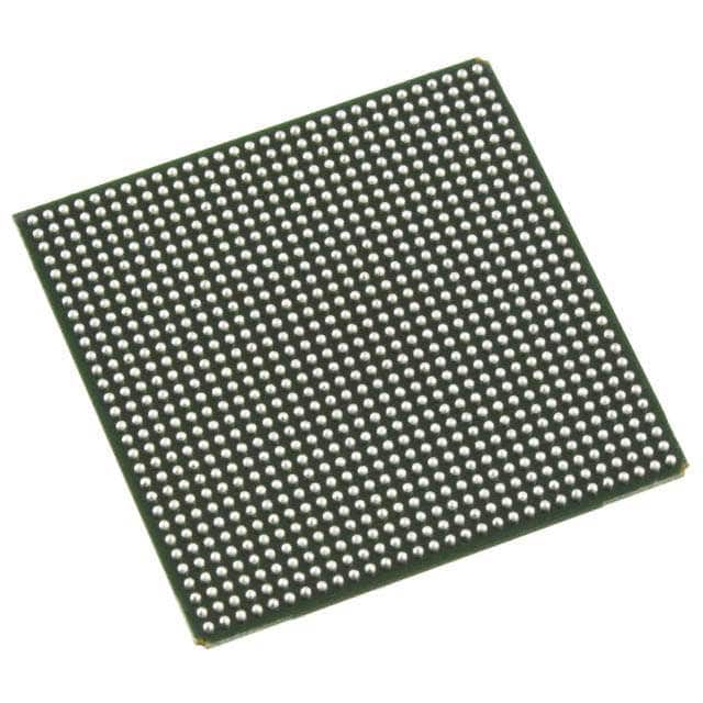
Package
The LFE2M70SE-6F900C comes in a compact and durable package suitable for surface mount technology (SMT) assembly.
Essence
The essence of this product lies in its ability to provide a customizable hardware platform that allows users to implement their own digital logic designs.
Packaging/Quantity
The LFE2M70SE-6F900C is typically packaged in reels or trays, with each reel containing a specific quantity of units. The exact packaging and quantity may vary depending on the manufacturer's specifications.
Specifications
- FPGA Family: Lattice ECP2M
- Logic Elements: 70,000
- Speed Grade: 6
- Operating Voltage: 1.2V
- I/O Pins: 900
- Embedded Memory: 4.8 Mb
- Maximum Frequency: 400 MHz
- Package Type: FBGA
- Package Pins: 900
Detailed Pin Configuration
The pin configuration of the LFE2M70SE-6F900C FPGA is as follows:
- Pin 1: VCCIO
- Pin 2: GND
- Pin 3: VCCINT
- Pin 4: GND
- Pin 5: IOB_0
- Pin 6: IOB_1
- ...
- Pin 900: IOB_899
Functional Features
- High-speed performance with low power consumption
- Configurable I/O standards and voltage levels
- Embedded memory blocks for efficient data storage
- Dedicated clock management resources
- Support for various communication protocols
- Flexible routing architecture for complex designs
Advantages and Disadvantages
Advantages
- Versatile and customizable platform for digital logic design
- High-performance capabilities suitable for demanding applications
- Low power consumption for energy-efficient operation
- Large capacity to accommodate complex designs
- Wide range of I/O options for connectivity
Disadvantages
- Steep learning curve for beginners due to the complexity of FPGA programming
- Higher cost compared to traditional microcontrollers or ASICs
- Limited availability of alternative models from other manufacturers
Working Principles
The LFE2M70SE-6F900C FPGA operates based on the principles of reconfigurable hardware. It consists of a matrix of configurable logic elements interconnected through programmable routing resources. Users can program the FPGA using Hardware Description Languages (HDL) such as VHDL or Verilog to define the desired functionality. The programmed configuration is then loaded into the FPGA, allowing it to perform the specified operations.
Detailed Application Field Plans
The LFE2M70SE-6F900C FPGA finds application in various fields, including:
- Telecommunications: Used in base stations, network switches, and routers for high-speed data processing and protocol handling.
- Automotive: Employed in advanced driver assistance systems (ADAS), engine control units (ECUs), and infotainment systems for enhanced functionality and performance.
- Industrial Automation: Utilized in programmable logic controllers (PLCs), motor control systems, and robotics for precise control and automation.
- Consumer Electronics: Integrated into smart TVs, gaming consoles, and wearable devices to enable advanced features and connectivity.
Detailed and Complete Alternative Models
While the LFE2M70SE-6F900C is a high-performance FPGA, there are alternative models available from other manufacturers that offer similar capabilities. Some notable alternatives include:
- Xilinx Virtex UltraScale+: Offers comparable performance and capacity with advanced features such as integrated high-speed transceivers.
- Intel Cyclone V: Provides a cost-effective solution with a wide range of I/O options and embedded memory blocks.
- Microchip PolarFire: Known for its low power consumption and security features, suitable for applications requiring high reliability.
In conclusion, the LFE2M70SE-6F900C FPGA is a versatile and powerful device that enables users to implement complex digital logic designs. With its high-performance capabilities and flexible architecture, it finds application in various fields, including telecommunications, automotive, industrial automation, and consumer electronics. While it has advantages such as customization and low power consumption, it also has disadvantages like a steep learning curve and higher cost compared to other options. Nonetheless, the LFE2M70SE-6F900C remains a popular choice for professionals seeking a reliable FPGA solution.
Listen Sie 10 häufige Fragen und Antworten im Zusammenhang mit der Anwendung von LFE2M70SE-6F900C in technischen Lösungen auf
Sure! Here are 10 common questions and answers related to the application of LFE2M70SE-6F900C in technical solutions:
Q: What is the LFE2M70SE-6F900C? A: The LFE2M70SE-6F900C is a specific model of Field-Programmable Gate Array (FPGA) manufactured by Lattice Semiconductor.
Q: What are the key features of the LFE2M70SE-6F900C? A: The LFE2M70SE-6F900C offers 70,000 Look-Up Tables (LUTs), 1,152 Kbits of embedded memory, 360 programmable I/O pins, and operates at a maximum frequency of 900 MHz.
Q: What are some typical applications for the LFE2M70SE-6F900C? A: The LFE2M70SE-6F900C is commonly used in various technical solutions such as telecommunications, industrial automation, automotive electronics, medical devices, and aerospace systems.
Q: How can I program the LFE2M70SE-6F900C? A: The LFE2M70SE-6F900C can be programmed using Lattice Diamond design software or other compatible programming tools provided by Lattice Semiconductor.
Q: What is the power supply requirement for the LFE2M70SE-6F900C? A: The LFE2M70SE-6F900C requires a single power supply voltage of 1.2V.
Q: Can I interface the LFE2M70SE-6F900C with other components or microcontrollers? A: Yes, the LFE2M70SE-6F900C supports various communication interfaces such as SPI, I2C, UART, and GPIOs, allowing easy integration with other components or microcontrollers.
Q: What are the temperature operating ranges for the LFE2M70SE-6F900C? A: The LFE2M70SE-6F900C can operate within a temperature range of -40°C to +100°C.
Q: Does the LFE2M70SE-6F900C support security features? A: Yes, the LFE2M70SE-6F900C provides built-in security features like bitstream encryption and authentication to protect against unauthorized access or tampering.
Q: Can I use the LFE2M70SE-6F900C for high-speed data processing? A: Absolutely! The LFE2M70SE-6F900C's high maximum frequency of 900 MHz makes it suitable for applications requiring fast data processing and real-time operations.
Q: Where can I find additional technical documentation and support for the LFE2M70SE-6F900C? A: You can find detailed datasheets, application notes, reference designs, and support resources on the official website of Lattice Semiconductor or by contacting their customer support team.