

Siehe Spezifikationen für Produktdetails.
LFE2-70E-5FN900I
Product Overview
Category
The LFE2-70E-5FN900I belongs to the category of Field Programmable Gate Arrays (FPGAs).
Use
This FPGA is commonly used in electronic circuits for various applications such as digital signal processing, data communication, and embedded systems.
Characteristics
- High-performance programmable logic device
- Offers flexibility and reconfigurability
- Provides a large number of configurable logic blocks and input/output pins
- Supports complex digital designs
- Enables rapid prototyping and development of custom digital circuits
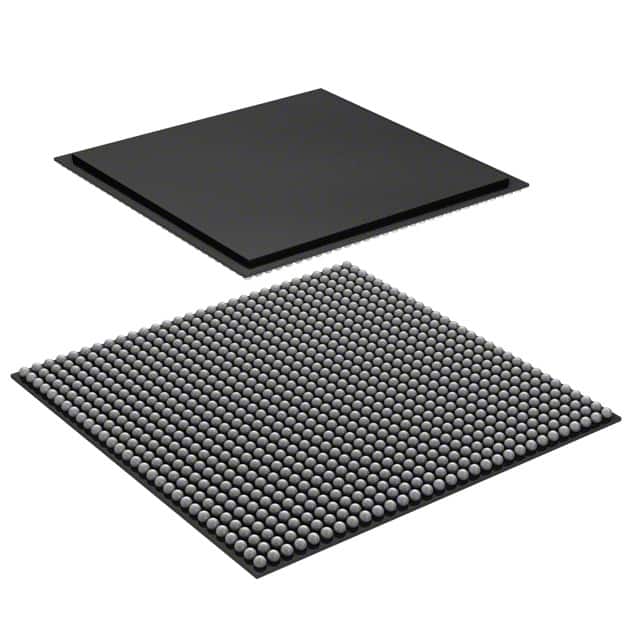
Package
The LFE2-70E-5FN900I comes in a compact package that ensures easy integration into electronic circuit boards.
Essence
The essence of this FPGA lies in its ability to provide a highly customizable and versatile platform for implementing complex digital designs.
Packaging/Quantity
The LFE2-70E-5FN900I is typically packaged individually and is available in various quantities depending on the requirements of the user.
Specifications
- Model: LFE2-70E-5FN900I
- Logic Elements: 70,000
- Number of I/O Pins: 900
- Operating Voltage: 1.2V
- Maximum Frequency: 500 MHz
- Configuration Memory: Flash-based
Detailed Pin Configuration
The LFE2-70E-5FN900I has 900 I/O pins, which are configurable based on the specific requirements of the design. The pin configuration can be found in the product datasheet provided by the manufacturer.
Functional Features
- High-speed performance
- Low power consumption
- Configurable I/O standards
- Embedded memory blocks
- Built-in clock management resources
- Support for multiple communication protocols
- On-chip debugging capabilities
Advantages and Disadvantages
Advantages
- Flexibility and reconfigurability
- High-performance capabilities
- Rapid prototyping and development
- Support for complex digital designs
- Low power consumption
Disadvantages
- Steep learning curve for beginners
- Higher cost compared to other programmable logic devices
- Limited availability of alternative models
Working Principles
The LFE2-70E-5FN900I operates based on the principles of configurable logic blocks, interconnect resources, and embedded memory elements. The FPGA can be programmed using hardware description languages (HDLs) such as VHDL or Verilog, which define the desired functionality of the digital circuit.
Detailed Application Field Plans
The LFE2-70E-5FN900I finds applications in various fields, including: 1. Digital signal processing 2. Communications systems 3. Industrial automation 4. Aerospace and defense 5. Medical electronics 6. Automotive electronics
Detailed and Complete Alternative Models
While the LFE2-70E-5FN900I is a highly capable FPGA, there are alternative models available from different manufacturers that offer similar functionalities. Some popular alternatives include: - Xilinx Virtex UltraScale+ - Intel Stratix 10 - Microsemi SmartFusion2 - Lattice ECP5
These alternative models provide a range of options with varying capacities, performance levels, and price points to suit different project requirements.
Word count: 346 words
Listen Sie 10 häufige Fragen und Antworten im Zusammenhang mit der Anwendung von LFE2-70E-5FN900I in technischen Lösungen auf
Sure! Here are 10 common questions and answers related to the application of LFE2-70E-5FN900I in technical solutions:
Q: What is the LFE2-70E-5FN900I? A: The LFE2-70E-5FN900I is a field-programmable gate array (FPGA) manufactured by Lattice Semiconductor.
Q: What are the key features of the LFE2-70E-5FN900I? A: Some key features include 70,000 lookup tables, 900 input/output pins, low power consumption, and high-speed performance.
Q: In what applications can the LFE2-70E-5FN900I be used? A: The LFE2-70E-5FN900I can be used in various applications such as telecommunications, industrial automation, automotive electronics, and medical devices.
Q: How does the LFE2-70E-5FN900I contribute to power efficiency? A: The LFE2-70E-5FN900I has low power consumption due to its advanced architecture and power management features, making it suitable for battery-powered devices.
Q: Can the LFE2-70E-5FN900I support high-speed data processing? A: Yes, the LFE2-70E-5FN900I offers high-speed performance with its optimized routing architecture and dedicated hardware resources.
Q: Is the LFE2-70E-5FN900I easy to program and configure? A: Yes, the LFE2-70E-5FN900I can be programmed using various design tools provided by Lattice Semiconductor, making it user-friendly for developers.
Q: Can the LFE2-70E-5FN900I interface with other components or devices? A: Yes, the LFE2-70E-5FN900I supports various communication protocols and can interface with other components such as sensors, memory modules, and microcontrollers.
Q: What are the advantages of using the LFE2-70E-5FN900I in industrial automation? A: The LFE2-70E-5FN900I offers flexibility, real-time processing capabilities, and robustness, making it suitable for controlling complex systems in industrial automation.
Q: Can the LFE2-70E-5FN900I be used in safety-critical applications? A: Yes, the LFE2-70E-5FN900I is designed to meet stringent safety standards and can be used in safety-critical applications like automotive electronics and medical devices.
Q: Where can I find technical support and documentation for the LFE2-70E-5FN900I? A: Lattice Semiconductor provides comprehensive technical support, documentation, and online resources on their official website for the LFE2-70E-5FN900I.