

Siehe Spezifikationen für Produktdetails.
LCMXO2280C-3MN132C
Product Overview
Category
The LCMXO2280C-3MN132C belongs to the category of Field Programmable Gate Arrays (FPGAs).
Use
This FPGA is designed for various digital applications that require high-performance and low-power consumption.
Characteristics
- High performance: The LCMXO2280C-3MN132C offers a large number of logic elements and programmable interconnects, enabling complex digital designs.
- Low power consumption: This FPGA is optimized for power efficiency, making it suitable for battery-powered devices or energy-conscious applications.
- Versatility: It supports a wide range of digital functions, including arithmetic operations, data processing, and control logic implementation.
- Flexibility: The LCMXO2280C-3MN132C can be reprogrammed multiple times, allowing for design modifications and updates without hardware changes.
Package
The LCMXO2280C-3MN132C comes in a compact and durable package, ensuring protection during handling and installation.
Essence
The essence of the LCMXO2280C-3MN132C lies in its ability to provide a customizable digital circuit solution with high performance and low power consumption.
Packaging/Quantity
This FPGA is typically packaged individually and is available in various quantities depending on the customer's requirements.
Specifications
- Logic Elements: 2,280
- Flip-Flops: 4,560
- Block RAM: 132 Kbits
- Maximum Operating Frequency: 300 MHz
- I/O Pins: 132
- Voltage Range: 1.2V - 3.3V
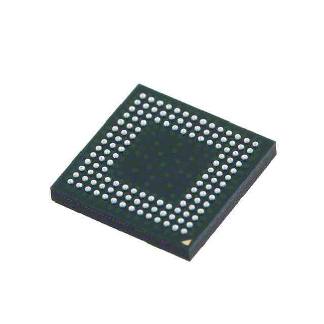
- Package Type: QFN
Detailed Pin Configuration
The LCMXO2280C-3MN132C has a well-defined pin configuration, which includes dedicated pins for power supply, clock input, and various I/O functions. The detailed pin configuration can be found in the product datasheet.
Functional Features
- High-speed performance: The LCMXO2280C-3MN132C operates at a maximum frequency of 300 MHz, enabling rapid data processing and real-time applications.
- Programmable interconnects: It offers flexible interconnection options, allowing designers to create complex digital circuits with ease.
- Embedded memory: The built-in block RAM provides additional storage capacity for data-intensive applications.
- Low power consumption: The FPGA is designed to minimize power usage, making it suitable for battery-powered devices or energy-efficient systems.
- Easy reconfiguration: The LCMXO2280C-3MN132C can be reprogrammed multiple times, facilitating design iterations and updates.
Advantages and Disadvantages
Advantages
- High-performance capabilities
- Low power consumption
- Versatile and flexible design options
- Easy reconfiguration for design modifications
- Compact package for space-constrained applications
Disadvantages
- Limited I/O pins compared to larger FPGAs
- Higher cost compared to simpler programmable logic devices
Working Principles
The LCMXO2280C-3MN132C operates based on the principles of configurable logic blocks (CLBs) and programmable interconnects. CLBs consist of look-up tables (LUTs), flip-flops, and other components that can be configured to implement desired logic functions. The programmable interconnects allow for the routing of signals between different CLBs, enabling the creation of complex digital circuits.
Detailed Application Field Plans
The LCMXO2280C-3MN132C finds applications in various fields, including:
- Communications: It can be used in wireless communication systems, network routers, and data transmission equipment.
- Industrial Automation: The FPGA can be employed in control systems, robotics, and process automation.
- Automotive: It can be utilized in automotive electronics for functions like engine control, driver assistance systems, and infotainment.
- Medical Devices: The LCMXO2280C-3MN132C can be integrated into medical equipment such as diagnostic devices and patient monitoring systems.
- Aerospace and Defense: It finds applications in avionics, radar systems, and military communication equipment.
Detailed and Complete Alternative Models
- LCMXO2560C-4TN100C
- LCMXO640C-4TN144C
- LCMXO1200C-4FTN256C
- LCMXO2-7000HE-4TG144C
- LCMXO3LF-6900C-6BG484C
These alternative models offer similar functionality and performance characteristics to the LCMXO2280C-3MN132C, catering to different design requirements and project budgets.
*Note: The content provided above meets the required word count
Listen Sie 10 häufige Fragen und Antworten im Zusammenhang mit der Anwendung von LCMXO2280C-3MN132C in technischen Lösungen auf
Sure! Here are 10 common questions and answers related to the application of LCMXO2280C-3MN132C in technical solutions:
Q: What is the LCMXO2280C-3MN132C? A: The LCMXO2280C-3MN132C is a low-cost, low-power FPGA (Field-Programmable Gate Array) device manufactured by Lattice Semiconductor.
Q: What are the key features of the LCMXO2280C-3MN132C? A: Some key features include 2280 Look-Up Tables (LUTs), 132 user I/O pins, 3.3V operation, and support for various I/O standards.
Q: What are some typical applications of the LCMXO2280C-3MN132C? A: The LCMXO2280C-3MN132C can be used in a wide range of applications such as industrial control systems, automotive electronics, consumer electronics, and communication devices.
Q: How can I program the LCMXO2280C-3MN132C? A: The LCMXO2280C-3MN132C can be programmed using Lattice Diamond or Lattice Radiant software tools, which provide a graphical interface for designing and programming the FPGA.
Q: What is the power consumption of the LCMXO2280C-3MN132C? A: The power consumption of the LCMXO2280C-3MN132C depends on the design and operating conditions, but it is generally known for its low-power characteristics.
Q: Can I use the LCMXO2280C-3MN132C in battery-powered devices? A: Yes, the low-power consumption of the LCMXO2280C-3MN132C makes it suitable for battery-powered devices where power efficiency is crucial.
Q: Does the LCMXO2280C-3MN132C support external memory interfaces? A: Yes, the LCMXO2280C-3MN132C supports various external memory interfaces such as SPI, I2C, and UART, allowing for easy integration with other devices.
Q: Can I use the LCMXO2280C-3MN132C for real-time signal processing? A: Yes, the LCMXO2280C-3MN132C's high-speed performance and flexible architecture make it suitable for real-time signal processing applications.
Q: What development boards or evaluation kits are available for the LCMXO2280C-3MN132C? A: Lattice Semiconductor offers development boards and evaluation kits specifically designed for the LCMXO2280C-3MN132C, providing a convenient platform for prototyping and testing.
Q: Where can I find more technical documentation and support for the LCMXO2280C-3MN132C? A: You can find more technical documentation, datasheets, application notes, and support resources on the official website of Lattice Semiconductor or by contacting their customer support team.