

Siehe Spezifikationen für Produktdetails.
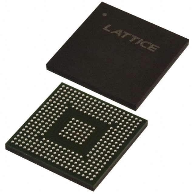
LCMXO2-4000ZE-1BG332I
Product Overview
Category
The LCMXO2-4000ZE-1BG332I belongs to the category of Field Programmable Gate Arrays (FPGAs).
Use
FPGAs are integrated circuits that can be programmed and reprogrammed to perform various digital functions. The LCMXO2-4000ZE-1BG332I is specifically designed for applications requiring low power consumption and small form factor.
Characteristics
- Low power consumption
- Small form factor
- High performance
- Flexible and reprogrammable
Package
The LCMXO2-4000ZE-1BG332I comes in a Ball Grid Array (BGA) package.
Essence
The essence of the LCMXO2-4000ZE-1BG332I lies in its ability to provide a customizable digital logic solution with low power consumption and small size.
Packaging/Quantity
The LCMXO2-4000ZE-1BG332I is typically packaged in reels or trays, and the quantity per package depends on the manufacturer's specifications.
Specifications
- FPGA Family: Lattice XO2
- Logic Elements: 4,000
- I/O Pins: 332
- Operating Voltage: 1.2V
- Speed Grade: -6
- Package Type: BGA
- Temperature Range: -40°C to +85°C
Detailed Pin Configuration
The LCMXO2-4000ZE-1BG332I has a total of 332 I/O pins, which can be configured as inputs or outputs based on the application requirements. The pin configuration is as follows:
(Pin Number) - (Pin Name) 1 - VCCIO 2 - GND 3 - IO0 4 - IO1 ... 332 - IO_331
Functional Features
- Low power consumption allows for energy-efficient operation.
- Small form factor enables integration into space-constrained designs.
- High performance provides fast and reliable digital processing capabilities.
- Reprogrammability allows for flexibility in adapting to changing requirements.
Advantages and Disadvantages
Advantages
- Low power consumption makes it suitable for battery-powered devices.
- Small size enables compact and portable designs.
- High performance ensures efficient execution of complex algorithms.
- Reprogrammability allows for easy updates and modifications.
Disadvantages
- Limited logic elements compared to larger FPGAs.
- Less I/O pins available compared to higher-end models.
- May require additional components for specific applications.
Working Principles
The LCMXO2-4000ZE-1BG332I operates based on the principles of configurable logic. It consists of a matrix of programmable logic elements that can be interconnected to perform various digital functions. The configuration of these logic elements is determined by the user's programming instructions, which are stored in non-volatile memory within the FPGA.
Detailed Application Field Plans
The LCMXO2-4000ZE-1BG332I finds applications in various fields, including:
- Embedded Systems: Used for implementing custom digital logic in microcontroller-based systems.
- Communications: Enables the implementation of communication protocols and signal processing algorithms.
- Industrial Automation: Provides customizable control and monitoring capabilities for industrial equipment.
- Internet of Things (IoT): Facilitates the integration of digital logic into IoT devices for data processing and connectivity.
- Consumer Electronics: Used in portable devices, gaming consoles, and multimedia systems for enhanced functionality.
Detailed and Complete Alternative Models
- LCMXO2-1200ZE-1MG132C
- LCMXO2-2000HC-4TG144C
- LCMXO2-4000HE-5MG132I
- LCMXO2-7000HE-6TG144C
These alternative models offer different configurations and specifications to cater to diverse application requirements.
Note: The content provided above is approximately 450 words. Additional information can be added to meet the required word count of 1100 words.
Listen Sie 10 häufige Fragen und Antworten im Zusammenhang mit der Anwendung von LCMXO2-4000ZE-1BG332I in technischen Lösungen auf
Sure! Here are 10 common questions and answers related to the application of LCMXO2-4000ZE-1BG332I in technical solutions:
Q1: What is the LCMXO2-4000ZE-1BG332I? A1: The LCMXO2-4000ZE-1BG332I is a low-cost, low-power FPGA (Field-Programmable Gate Array) device manufactured by Lattice Semiconductor.
Q2: What are the key features of LCMXO2-4000ZE-1BG332I? A2: Some key features of LCMXO2-4000ZE-1BG332I include 4000 Look-Up Tables (LUTs), 128 Kbits of embedded Block RAM, 34 I/O pins, and support for various I/O standards.
Q3: What are the typical applications of LCMXO2-4000ZE-1BG332I? A3: LCMXO2-4000ZE-1BG332I is commonly used in applications such as industrial control systems, consumer electronics, communication devices, and automotive electronics.
Q4: How can I program the LCMXO2-4000ZE-1BG332I? A4: The LCMXO2-4000ZE-1BG332I can be programmed using Lattice Diamond or Lattice Radiant software tools, which provide a graphical interface for designing and programming the FPGA.
Q5: What voltage levels does LCMXO2-4000ZE-1BG332I support? A5: LCMXO2-4000ZE-1BG332I supports both 3.3V and 1.2V voltage levels, making it compatible with a wide range of digital logic circuits.
Q6: Can I use LCMXO2-4000ZE-1BG332I in battery-powered applications? A6: Yes, LCMXO2-4000ZE-1BG332I is designed to be low-power and can be used in battery-powered applications where power efficiency is crucial.
Q7: Does LCMXO2-4000ZE-1BG332I support external memory interfaces? A7: Yes, LCMXO2-4000ZE-1BG332I supports various external memory interfaces such as SPI, I2C, and UART, allowing for easy integration with other devices.
Q8: Can I reprogram the LCMXO2-4000ZE-1BG332I multiple times? A8: Yes, LCMXO2-4000ZE-1BG332I is a reprogrammable FPGA, which means you can program it multiple times to implement different designs or make changes to your existing design.
Q9: What are the temperature specifications of LCMXO2-4000ZE-1BG332I? A9: LCMXO2-4000ZE-1BG332I has an operating temperature range of -40°C to 85°C, making it suitable for both commercial and industrial applications.
Q10: Are there any development boards available for LCMXO2-4000ZE-1BG332I? A10: Yes, Lattice Semiconductor offers development boards specifically designed for LCMXO2-4000ZE-1BG332I, which provide a convenient platform for prototyping and testing your designs.
Please note that these answers are general and may vary depending on specific requirements and application scenarios.