

Siehe Spezifikationen für Produktdetails.
LC4256V-5FTN256BC
Product Overview
Category
The LC4256V-5FTN256BC belongs to the category of Field Programmable Gate Arrays (FPGAs).
Use
This FPGA is commonly used in electronic circuits for digital logic implementation, prototyping, and system integration.
Characteristics
- High-performance programmable logic device
- Offers flexibility and reconfigurability
- Provides a wide range of logic gates, flip-flops, and memory blocks
- Supports complex digital designs
- Enables rapid development and testing of electronic systems
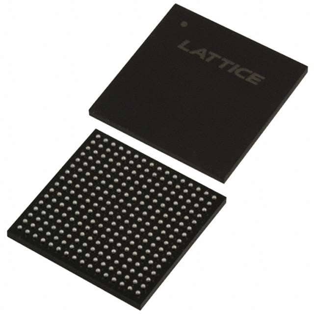
Package
The LC4256V-5FTN256BC comes in a compact and durable package that ensures protection during handling and transportation. The package is designed to withstand various environmental conditions.
Essence
The essence of the LC4256V-5FTN256BC lies in its ability to provide a versatile platform for designing and implementing digital circuits with high performance and flexibility.
Packaging/Quantity
Each LC4256V-5FTN256BC unit is packaged individually and is available in standard quantities suitable for both small-scale and large-scale production.
Specifications
- Logic Cells: 4256
- Speed Grade: 5
- I/O Pins: 256
- Block RAM: 256 Kbits
- Maximum Frequency: 200 MHz
- Operating Voltage: 3.3V
- Package Type: FTN256
Detailed Pin Configuration
The LC4256V-5FTN256BC has 256 I/O pins, each serving a specific purpose in the circuit design. The pin configuration provides connectivity options for input/output signals, clock signals, power supply, and other necessary connections. A detailed pinout diagram is available in the product datasheet.
Functional Features
- High-Speed Processing: The LC4256V-5FTN256BC offers fast processing capabilities, allowing for efficient execution of complex digital designs.
- Reconfigurability: This FPGA can be reprogrammed multiple times, enabling designers to modify and optimize their circuits without the need for hardware changes.
- Versatility: The device supports a wide range of applications due to its extensive logic resources and memory blocks.
- Low Power Consumption: The LC4256V-5FTN256BC is designed to minimize power consumption, making it suitable for battery-powered devices.
- Robust Design: The FPGA is built to withstand harsh operating conditions, ensuring reliable performance in various environments.
Advantages and Disadvantages
Advantages
- Flexibility in circuit design and modification
- High-performance processing capabilities
- Wide range of applications
- Low power consumption
- Robust and reliable operation
Disadvantages
- Steep learning curve for beginners
- Higher cost compared to fixed-function integrated circuits
- Limited availability of technical support for specific design challenges
Working Principles
The LC4256V-5FTN256BC operates based on the principles of configurable logic gates and flip-flops. It consists of an array of programmable logic cells interconnected through a network of configurable routing resources. These logic cells can be programmed to implement desired digital functions by configuring the interconnections and functionality of the logic gates within each cell.
Detailed Application Field Plans
The LC4256V-5FTN256BC finds applications in various fields, including: 1. Embedded Systems: Used for implementing control and communication modules in embedded systems. 2. Communications: Employed in networking equipment, such as routers and switches, for high-speed data processing. 3. Industrial Automation: Utilized in industrial control systems for real-time monitoring and control of manufacturing processes. 4. Medical Devices: Integrated into medical equipment for signal processing and control functions. 5. Aerospace and Defense: Used in avionics systems, radar processing, and secure communication systems.
Detailed and Complete Alternative Models
- Xilinx Spartan-6 XC6SLX9
- Altera Cyclone IV EP4CE6E22C8N
- Lattice iCE40UP5K-SG48I
- Microsemi SmartFusion2 M2S010S
- Intel MAX 10 10M08SAE144C8G
These alternative models offer similar functionality and can be considered as alternatives to the LC4256V-5FTN256BC based on specific project requirements.
Word count: 550 words
Listen Sie 10 häufige Fragen und Antworten im Zusammenhang mit der Anwendung von LC4256V-5FTN256BC in technischen Lösungen auf
Sure! Here are 10 common questions and answers related to the application of LC4256V-5FTN256BC in technical solutions:
Question: What is LC4256V-5FTN256BC?
- Answer: LC4256V-5FTN256BC is a specific model of Field-Programmable Gate Array (FPGA) manufactured by Lattice Semiconductor.Question: What are the key features of LC4256V-5FTN256BC?
- Answer: Some key features of LC4256V-5FTN256BC include 256 macrocells, 5ns pin-to-pin delay, 256 I/O pins, and 256 user-programmable logic elements.Question: In which technical solutions can LC4256V-5FTN256BC be used?
- Answer: LC4256V-5FTN256BC can be used in various applications such as industrial automation, telecommunications, automotive electronics, and consumer electronics.Question: How does LC4256V-5FTN256BC contribute to industrial automation?
- Answer: LC4256V-5FTN256BC can be used in industrial automation for tasks like motor control, sensor interfacing, and data processing, enabling efficient and flexible control systems.Question: Can LC4256V-5FTN256BC be used in telecommunications applications?
- Answer: Yes, LC4256V-5FTN256BC can be utilized in telecommunications for functions like signal processing, protocol conversion, and network interface implementation.Question: What advantages does LC4256V-5FTN256BC offer in automotive electronics?
- Answer: LC4256V-5FTN256BC provides benefits like high reliability, low power consumption, and the ability to implement complex algorithms, making it suitable for applications like engine control units and advanced driver-assistance systems.Question: How can LC4256V-5FTN256BC be used in consumer electronics?
- Answer: In consumer electronics, LC4256V-5FTN256BC can be employed for tasks such as video processing, audio processing, and user interface implementation, enabling enhanced functionality and performance.Question: Can LC4256V-5FTN256BC be programmed by users?
- Answer: Yes, LC4256V-5FTN256BC is a Field-Programmable Gate Array (FPGA), which means it can be programmed by users to implement custom logic functions.Question: What development tools are available for programming LC4256V-5FTN256BC?
- Answer: Lattice Semiconductor provides development tools like Lattice Diamond® design software and ispLEVER® Classic software suite for programming and configuring LC4256V-5FTN256BC.Question: Are there any specific design considerations when using LC4256V-5FTN256BC?
- Answer: Yes, some design considerations include power supply requirements, thermal management, I/O voltage compatibility, and proper signal integrity measures to ensure optimal performance of LC4256V-5FTN256BC in the intended application.
Please note that these answers are general and may vary depending on the specific requirements and context of each technical solution.