

Siehe Spezifikationen für Produktdetails.
IXFK150N15
Introduction
IXFK150N15 is a power MOSFET belonging to the category of electronic components. This semiconductor device is widely used in various applications due to its unique characteristics and functional features.
Basic Information Overview
- Category: Power MOSFET
- Use: Switching and amplification in electronic circuits
- Characteristics: High voltage capability, low on-resistance, fast switching speed
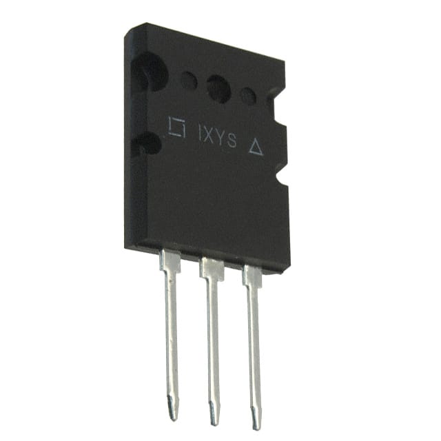
- Package: TO-264
- Essence: Semiconductor device for power management
- Packaging/Quantity: Typically sold in reels or tubes containing multiple units
Specifications
- Voltage Rating: 150V
- Current Rating: 15A
- On-Resistance: Low (typically in milliohms)
- Gate Threshold Voltage: Varies based on manufacturer specifications
- Operating Temperature Range: -55°C to 175°C
Detailed Pin Configuration
The IXFK150N15 typically has three pins: 1. Gate (G): Controls the conductivity between the source and drain terminals. 2. Source (S): Connected to the ground or common reference point. 3. Drain (D): Carries the current when the MOSFET is in the conducting state.
Functional Features
- High Voltage Capability: Suitable for high-power applications.
- Low On-Resistance: Minimizes power loss and heat generation.
- Fast Switching Speed: Enables rapid switching in electronic circuits.
Advantages and Disadvantages
Advantages
- Efficient power management
- Reduced heat dissipation
- Fast response time
Disadvantages
- Sensitivity to static electricity
- Potential for gate oxide damage if mishandled
Working Principles
The IXFK150N15 operates based on the principles of field-effect transistors, where the voltage applied to the gate terminal controls the flow of current between the source and drain terminals. When the gate-source voltage exceeds the threshold, the MOSFET enters the conducting state, allowing current to flow through.
Detailed Application Field Plans
The IXFK150N15 finds extensive use in the following application fields: - Switching Power Supplies: Efficiently regulate power flow in electronic devices. - Motor Control: Drive motors with precise control and minimal energy loss. - Inverters: Convert DC power to AC power in renewable energy systems.
Detailed and Complete Alternative Models
- IXFK120N15: Lower voltage rating with similar characteristics.
- IXFK150P15: Complementary P-channel MOSFET for specific circuit configurations.
- IXFK150N20: Higher voltage rating for applications requiring increased voltage tolerance.
In conclusion, the IXFK150N15 power MOSFET offers a balance of high voltage capability, low on-resistance, and fast switching speed, making it a versatile component in various electronic circuits and power management systems.
Word Count: 411
Listen Sie 10 häufige Fragen und Antworten im Zusammenhang mit der Anwendung von IXFK150N15 in technischen Lösungen auf
What is the maximum voltage rating of IXFK150N15?
- The maximum voltage rating of IXFK150N15 is 1500V.
What is the continuous drain current of IXFK150N15?
- The continuous drain current of IXFK150N15 is typically 150A.
What type of package does IXFK150N15 come in?
- IXFK150N15 comes in a TO-264 package.
What is the typical on-resistance of IXFK150N15?
- The typical on-resistance of IXFK150N15 is 0.15 ohms.
Is IXFK150N15 suitable for high-power applications?
- Yes, IXFK150N15 is suitable for high-power applications due to its high voltage and current ratings.
Does IXFK150N15 require a heatsink for proper operation?
- Yes, IXFK150N15 may require a heatsink for efficient heat dissipation, especially in high-power applications.
What are the typical applications of IXFK150N15?
- IXFK150N15 is commonly used in power supplies, motor drives, and other high-power switching applications.
What is the gate-source voltage range for IXFK150N15?
- The gate-source voltage range for IXFK150N15 is typically ±20V.
Can IXFK150N15 be used in parallel to increase current handling capability?
- Yes, IXFK150N15 can be used in parallel to increase current handling capability in certain applications.
What are the thermal characteristics of IXFK150N15?
- The thermal resistance from junction to case (RθJC) of IXFK150N15 is typically 0.35°C/W, indicating its ability to dissipate heat effectively.