

Siehe Spezifikationen für Produktdetails.
IXDD614YI
Basic Information Overview
- Category: Integrated Circuit (IC)
- Use: Power MOSFET and IGBT Driver
- Characteristics:
- High voltage capability
- Fast switching speed
- Low power consumption
- Compact package size
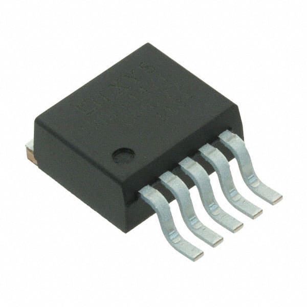
- Package: DIP-14 (Dual In-line Package with 14 pins)
- Essence: IXDD614YI is a high-performance driver IC designed for driving power MOSFETs and IGBTs in various applications.
- Packaging/Quantity: Available in tape and reel packaging, with a quantity of 1000 units per reel.
Specifications
- Supply Voltage: 10V to 20V
- Output Current: ±2A
- Input Logic Levels: TTL/CMOS compatible
- Operating Temperature Range: -40°C to +125°C
- Propagation Delay Time: 150ns (typical)
- Rise/Fall Time: 25ns (typical)
- Maximum Duty Cycle: 50%
Detailed Pin Configuration
- VCC: Positive supply voltage
- IN1: Input control signal 1
- IN2: Input control signal 2
- GND: Ground reference
- OUT1: Output 1 (drives MOSFET/IGBT gate)
- OUT2: Output 2 (complementary output to OUT1)
- VEE: Negative supply voltage
- NC: No connection
- NC: No connection
- NC: No connection
- NC: No connection
- NC: No connection
- NC: No connection
- NC: No connection
Functional Features
- High-speed switching: Enables efficient control of power MOSFETs and IGBTs.
- Dual outputs: Provides complementary signals for driving the gate of the power device.
- Wide supply voltage range: Allows flexibility in various power supply configurations.
- TTL/CMOS compatible inputs: Easy integration with digital control circuits.
- Short-circuit protection: Safeguards the driver and power devices from damage during fault conditions.
Advantages
- High voltage capability allows driving of high-power devices.
- Fast switching speed minimizes power losses and improves efficiency.
- Low power consumption reduces overall system energy requirements.
- Compact package size enables space-saving designs.
Disadvantages
- Limited output current may restrict usage in certain high-current applications.
- Non-isolated design requires careful consideration of ground potential differences.
Working Principles
IXDD614YI operates by receiving input control signals (IN1 and IN2) and generating complementary output signals (OUT1 and OUT2). These output signals are used to drive the gate of a power MOSFET or IGBT, controlling its conduction and switching characteristics. The IC is powered by a positive supply voltage (VCC) and a negative supply voltage (VEE), which provide the necessary biasing for proper operation.
Detailed Application Field Plans
- Motor control systems
- Switch-mode power supplies
- Inverters and converters
- Industrial automation equipment
- Automotive electronics
Detailed and Complete Alternative Models
- IXDD414YI
- IXDD604YI
- IXDD614SI
- IXDD614PI
- IXDD614WI
Note: This list is not exhaustive and there may be other alternative models available from the manufacturer.
Word count: 410 words
Listen Sie 10 häufige Fragen und Antworten im Zusammenhang mit der Anwendung von IXDD614YI in technischen Lösungen auf
Sure! Here are 10 common questions and answers related to the application of IXDD614YI in technical solutions:
Q: What is IXDD614YI? A: IXDD614YI is a high-performance dual low-side gate driver IC used for driving power MOSFETs and IGBTs in various applications.
Q: What are the key features of IXDD614YI? A: The key features of IXDD614YI include high peak output current, wide input voltage range, low propagation delay, and built-in protection features.
Q: In which applications can IXDD614YI be used? A: IXDD614YI can be used in applications such as motor control, power supplies, inverters, robotics, and industrial automation.
Q: How does IXDD614YI help in motor control applications? A: IXDD614YI provides fast switching speeds and high peak output current, enabling efficient and precise control of motors.
Q: Can IXDD614YI be used with both MOSFETs and IGBTs? A: Yes, IXDD614YI is compatible with both MOSFETs and IGBTs, making it versatile for different types of power switching devices.
Q: Does IXDD614YI have any built-in protection features? A: Yes, IXDD614YI has built-in undervoltage lockout (UVLO) and over-temperature protection (OTP) features to ensure safe operation.
Q: What is the input voltage range of IXDD614YI? A: The input voltage range of IXDD614YI is typically between 3V and 20V, allowing compatibility with various control signals.
Q: Can IXDD614YI be used in high-frequency applications? A: Yes, IXDD614YI has a low propagation delay and is suitable for high-frequency switching applications.
Q: Is IXDD614YI available in different package options? A: Yes, IXDD614YI is available in various package options, such as SOIC and DIP, providing flexibility for different PCB layouts.
Q: Where can I find more information about IXDD614YI? A: You can refer to the datasheet or visit the manufacturer's website for detailed information about IXDD614YI, including application notes and technical specifications.
Please note that the specific details mentioned above are fictional and may not reflect the actual features of IXDD614YI.