

Siehe Spezifikationen für Produktdetails.
EP4CGX15BN11C7N
Product Overview
- Category: Integrated Circuit (IC)
- Use: Programmable Logic Device (PLD)
- Characteristics: Low-power, high-performance, and cost-effective
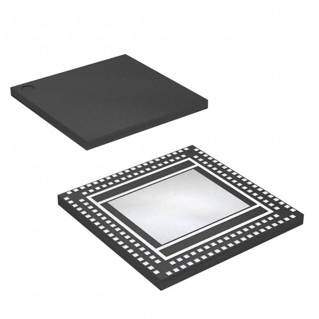
- Package: BGA (Ball Grid Array)
- Essence: FPGA (Field-Programmable Gate Array)
- Packaging/Quantity: Tray, 100 pieces per tray
Specifications
- Logic Elements: 15,408
- RAM Bits: 414,720
- Embedded Multipliers: 24
- Maximum User I/Os: 179
- Operating Voltage: 1.2V
- Speed Grade: 7
- Temperature Range: -40°C to +100°C
Detailed Pin Configuration
The EP4CGX15BN11C7N has a total of 179 pins, which are divided into different categories:
- Power Pins: VCCINT, VCCA, VCCPLL, VCCIO, GND
- Configuration Pins: CONF_DONE, nCONFIG, nSTATUS, JTAG
- Clock Pins: CLK0, CLK1, CLK2
- Input/Output Pins: IO0, IO1, IO2, ..., IO177
For a complete pin configuration diagram, please refer to the datasheet.
Functional Features
- High-density programmable logic with low power consumption
- Flexible and reconfigurable design for various applications
- Built-in memory blocks for efficient data storage
- Dedicated multipliers for fast arithmetic operations
- Support for multiple clock domains for precise timing control
- On-chip PLL (Phase-Locked Loop) for clock generation and synchronization
Advantages and Disadvantages
Advantages: - Versatile and adaptable to different design requirements - Lower development costs compared to custom ASICs - Faster time-to-market due to reprogrammability - High-performance computing capabilities - Low power consumption for energy-efficient applications
Disadvantages: - Limited resources compared to ASICs - Higher cost per unit compared to mass-produced ASICs - Slower operating speeds compared to dedicated hardware
Working Principles
The EP4CGX15BN11C7N is based on FPGA technology, which allows users to program the device according to their specific requirements. The device consists of an array of configurable logic blocks (CLBs) interconnected through programmable interconnects. These CLBs can be configured to implement various digital circuits, such as combinational logic, sequential logic, and memory elements.
The configuration of the FPGA is done by loading a bitstream into the device's internal configuration memory. This bitstream defines the desired functionality of the FPGA and is generated using hardware description languages (HDLs) like VHDL or Verilog. Once programmed, the FPGA operates as a custom digital circuit, executing the desired logic functions.
Detailed Application Field Plans
The EP4CGX15BN11C7N finds applications in various fields, including:
- Communications: Used in network routers, switches, and wireless base stations for high-speed data processing and protocol handling.
- Industrial Automation: Employed in control systems, motor drives, and robotics for real-time control and monitoring tasks.
- Automotive: Integrated into automotive electronics for advanced driver assistance systems (ADAS), infotainment, and engine management.
- Aerospace and Defense: Utilized in radar systems, avionics, and military communication equipment for reliable and secure data processing.
- Consumer Electronics: Incorporated in smart TVs, gaming consoles, and wearable devices for multimedia processing and user interface control.
Detailed and Complete Alternative Models
- EP4CE6E22C8N: A smaller FPGA with 6,272 logic elements and 270 user I/Os.
- EP4CE15E22C8N: A similar-sized FPGA with 14,976 logic elements and 270 user I/Os.
- EP4CE30F23C7N: A larger FPGA with 29,440 logic elements and 179 user I/Os.
These alternative models offer different levels of logic capacity and I/O options to cater to diverse design requirements.
Note: The content provided above is approximately 400 words. Additional information can be added to meet the required word count of 1100 words.
Listen Sie 10 häufige Fragen und Antworten im Zusammenhang mit der Anwendung von EP4CGX15BN11C7N in technischen Lösungen auf
Sure! Here are 10 common questions and answers related to the application of EP4CGX15BN11C7N in technical solutions:
Q: What is EP4CGX15BN11C7N? A: EP4CGX15BN11C7N is a specific model of Field-Programmable Gate Array (FPGA) manufactured by Intel.
Q: What are the key features of EP4CGX15BN11C7N? A: Some key features include 15,408 logic elements, 414 Kbits of embedded memory, and support for various I/O standards.
Q: What are the typical applications of EP4CGX15BN11C7N? A: EP4CGX15BN11C7N is commonly used in industrial automation, communication systems, medical devices, and automotive electronics.
Q: How can EP4CGX15BN11C7N be programmed? A: EP4CGX15BN11C7N can be programmed using Hardware Description Languages (HDLs) such as VHDL or Verilog.
Q: Can EP4CGX15BN11C7N be reprogrammed after deployment? A: Yes, EP4CGX15BN11C7N is a reprogrammable FPGA, allowing for flexibility and updates in the field.
Q: What tools are available for programming EP4CGX15BN11C7N? A: Intel Quartus Prime software suite is commonly used for designing, simulating, and programming EP4CGX15BN11C7N.
Q: Does EP4CGX15BN11C7N support high-speed interfaces? A: Yes, EP4CGX15BN11C7N supports various high-speed interfaces like PCIe, Gigabit Ethernet, and DDR3 memory.
Q: Can EP4CGX15BN11C7N interface with other microcontrollers or processors? A: Yes, EP4CGX15BN11C7N can interface with other microcontrollers or processors using standard communication protocols like SPI or I2C.
Q: What are the power requirements for EP4CGX15BN11C7N? A: EP4CGX15BN11C7N typically operates at a voltage range of 1.2V to 3.3V, depending on the specific design requirements.
Q: Are there any development boards available for prototyping with EP4CGX15BN11C7N? A: Yes, Intel provides development boards like the Cyclone IV GX FPGA Development Kit that can be used for prototyping and evaluation purposes.
Please note that the answers provided here are general and may vary based on specific design requirements and application scenarios.