

Siehe Spezifikationen für Produktdetails.
EP1S10F672C7N
Basic Information Overview
- Category: Programmable Logic Device (PLD)
- Use: EP1S10F672C7N is a PLD used for digital logic design and implementation.
- Characteristics:
- High-performance device with advanced features
- Large number of programmable logic elements
- Flexible I/O options
- Low power consumption
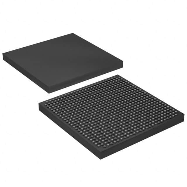
- Package: The EP1S10F672C7N comes in a compact package suitable for integration into various electronic systems.
- Essence: EP1S10F672C7N is designed to provide efficient and customizable digital logic solutions.
- Packaging/Quantity: The device is typically packaged individually and is available in various quantities depending on the manufacturer.
Specifications
- Number of Logic Elements: 10,000
- Maximum Frequency: 250 MHz
- Number of I/O Pins: 672
- Operating Voltage: 3.3V
- Technology: Field-Programmable Gate Array (FPGA)
Detailed Pin Configuration
The EP1S10F672C7N has a complex pin configuration with multiple input/output pins, power supply pins, and configuration pins. For a detailed pin configuration diagram, please refer to the manufacturer's datasheet.
Functional Features
- High-speed performance for demanding applications
- Extensive programmability for custom logic designs
- Support for various I/O standards and interfaces
- On-chip memory blocks for data storage
- Built-in clock management resources for precise timing control
Advantages and Disadvantages
Advantages: - Versatile and flexible for a wide range of applications - High-performance capabilities for complex designs - Lower power consumption compared to traditional logic implementations
Disadvantages: - Steep learning curve for beginners due to the complexity of FPGA programming - Higher cost compared to simpler logic devices
Working Principles
EP1S10F672C7N is based on FPGA technology, which allows for the reconfiguration of digital logic circuits. The device consists of programmable logic elements interconnected through configurable routing resources. These logic elements can be programmed to implement various functions and perform complex operations.
Detailed Application Field Plans
- Digital signal processing
- Communication systems
- Industrial automation
- Embedded systems
- Aerospace and defense applications
- High-performance computing
Detailed and Complete Alternative Models
- EP1S20F484C7N: Similar to EP1S10F672C7N but with higher logic capacity
- EP2S60F1020C5N: Advanced PLD with increased I/O pins and memory capacity
- EP3C120F780C7N: Latest generation FPGA with enhanced performance and features
Please note that the above alternative models are just a few examples, and there are many other options available in the market.
Word count: 315 words
Listen Sie 10 häufige Fragen und Antworten im Zusammenhang mit der Anwendung von EP1S10F672C7N in technischen Lösungen auf
Sure! Here are 10 common questions and answers related to the application of EP1S10F672C7N in technical solutions:
Q1: What is EP1S10F672C7N? A1: EP1S10F672C7N is a specific model of Field-Programmable Gate Array (FPGA) manufactured by Intel.
Q2: What are the key features of EP1S10F672C7N? A2: Some key features of EP1S10F672C7N include 672K logic elements, 10,752 Kbits of embedded memory, and support for various I/O standards.
Q3: What are the typical applications of EP1S10F672C7N? A3: EP1S10F672C7N is commonly used in applications such as industrial automation, telecommunications, automotive electronics, and high-performance computing.
Q4: How can EP1S10F672C7N be programmed? A4: EP1S10F672C7N can be programmed using Hardware Description Languages (HDLs) like VHDL or Verilog, along with design software provided by Intel.
Q5: Can EP1S10F672C7N be reprogrammed after initial programming? A5: Yes, EP1S10F672C7N is a reprogrammable FPGA, allowing for multiple iterations of designs and updates.
Q6: What kind of development tools are available for EP1S10F672C7N? A6: Intel provides Quartus Prime software suite, which includes design entry, synthesis, simulation, and programming tools for EP1S10F672C7N.
Q7: Does EP1S10F672C7N support different communication protocols? A7: Yes, EP1S10F672C7N supports various communication protocols such as PCIe, Ethernet, USB, and I2C, among others.
Q8: What is the power consumption of EP1S10F672C7N? A8: The power consumption of EP1S10F672C7N depends on the specific design and usage scenario. It is recommended to refer to the datasheet for detailed power specifications.
Q9: Can EP1S10F672C7N interface with external devices? A9: Yes, EP1S10F672C7N has a wide range of I/O pins that can be used to interface with external devices such as sensors, displays, and other peripherals.
Q10: Are there any reference designs or application notes available for EP1S10F672C7N? A10: Yes, Intel provides reference designs and application notes that can help users get started with EP1S10F672C7N and understand its implementation in different technical solutions.
Please note that the answers provided here are general and may vary based on specific requirements and documentation provided by Intel for EP1S10F672C7N.